- 您现在的位置:买卖IC网 > PDF目录19752 > TOP256GN-TL (Power Integrations)IC OFFLINE SWIT PROG OVP 8SMD PDF资料下载
参数资料
| 型号: | TOP256GN-TL |
| 厂商: | Power Integrations |
| 文件页数: | 23/50页 |
| 文件大小: | 0K |
| 描述: | IC OFFLINE SWIT PROG OVP 8SMD |
| 产品培训模块: | TOPSwitch® HX General Introduction |
| 标准包装: | 1 |
| 系列: | TOPSwitch®-HX |
| 输出隔离: | 隔离 |
| 频率范围: | 119kHz ~ 145kHz |
| 输出电压: | 700V |
| 功率(瓦特): | 63W |
| 工作温度: | -40°C ~ 150°C |
| 封装/外壳: | 8-SMD(7 个接脚),鸥形翼 |
| 供应商设备封装: | SMD-8C |
| 包装: | 标准包装 |
| 配用: | 596-1193-ND - KIT REF DESIGN TOP HX FOR TOP258 |
| 其它名称: | 596-1182-6 |
第1页第2页第3页第4页第5页第6页第7页第8页第9页第10页第11页第12页第13页第14页第15页第16页第17页第18页第19页第20页第21页第22页当前第23页第24页第25页第26页第27页第28页第29页第30页第31页第32页第33页第34页第35页第36页第37页第38页第39页第40页第41页第42页第43页第44页第45页第46页第47页第48页第49页第50页
�� �
�
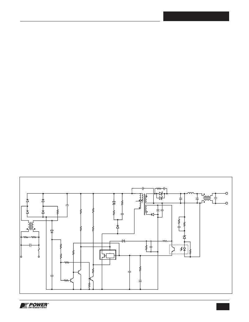
�TOP252-262�
�A� High� Efficiency,� 20� W� continuous� –� 80� W� Peak,� Universal�
�Input� Power� Supply�
�The� circuit� shown� in� Figure� 43� takes� advantage� of� several� of�
�TOPSwitch-HX� features� to� reduce� system� cost� and� power�
�supply� size� and� to� improve� power� supply� efficiency� while�
�delivering� significant� peak� power� for� a� short� duration.� This�
�design� delivers� continuous� 20� W� and� peak� 80� W� at� 32� V� from�
�an� 90� VAC� to� 264� VAC� input.� A� nominal� efficiency� of� 82%� at� full�
�load� is� achieved� using� TOP258MN.� The� M-package� part� has� an�
�optimized� current� limit� to� enable� design� of� power� supplies�
�capable� of� delivering� high� power� for� a� short� duration.�
�Resistor� R12� sets� the� current� limit� of� the� part.� Resistors� R11�
�and� R14� provide� line� feed� forward� information� that� reduces� the�
�current� limit� with� increasing� DC� bus� voltage,� thereby� maintaining�
�a� constant� overload� power� level� with� increasing� line� voltage.�
�Resistors� R1� and� R2� implement� the� line� undervoltage� and�
�overvoltage� function� and� also� provide� feed� forward� compensation�
�for� reducing� line� frequency� ripple� at� the� output.� The� overvoltage�
�feature� inhibits� TOPSwitch-HX� switching� during� a� line� surge�
�extending� the� high� voltage� withstand� to� 700� V� without� device�
�damage.�
�The� snubber� circuit� comprising� of� VR7,� R17,� R25,� C5� and� D2�
�limits� the� maximum� drain� voltage� and� dissipates� energy� stored� in�
�the� leakage� inductance� of� transformer� T1.� This� clamp� configuration�
�maximizes� energy� efficiency� by� preventing� C5� from� discharging�
�below� the� value� of� VR7� during� the� lower� frequency� operating�
�modes� of� TOPSwitch-HX.� Resistor� R25� damps� high� frequency�
�ringing� for� reduced� EMI.�
�A� combined� output� overvoltage� and� over� power� protection�
�circuit� is� provided� via� the� latching� shutdown� feature� of�
�TOPSwitch-HX� and� R20,� C9,� R22� and� VR5.� Should� the� bias�
�winding� output� voltage� across� C13� rise� due� to� output� overload�
�or� an� open� loop� fault� (opto� coupler� failure),� then� VR5� conducts�
�triggering� the� latching� shutdown.� To� prevent� false� triggering�
�due� to� short� duration� overload,� a� delay� is� provided� by� R20,� R22�
�and� C9.�
�To� reset� the� supply� following� a� latching� shutdown,� the� V� pin�
�must� fall� below� the� reset� threshold.� To� prevent� the� long� reset�
�delay� associated� with� the� input� capacitor� discharging,� a� fast� AC�
�reset� circuit� is� used.� The� AC� input� is� rectified� and� filtered� by�
�D13� and� C30.� While� the� AC� supply� is� present,� Q3� is� on� and� Q1�
�is� off,� allowing� normal� device� operation.� However� when� AC� is�
�removed,� Q1� pulls� down� the� V� pin� and� resets� the� latch.� The� supply�
�will� then� return� to� normal� operation� when� AC� is� again� applied.�
�Transistor� Q2� provides� an� additional� lower� UV� threshold� to� the�
�level� programmed� via� R1,� R2� and� the� V� pin.� At� low� input� AC�
�voltage,� Q2� turns� off,� allowing� the� X� pin� to� float� and� thereby�
�disabling� switching.�
�A� simple� feedback� circuit� automatically� regulates� the� output�
�voltage.� Zener� VR3� sets� the� output� voltage� together� with� the�
�voltage� drop� across� series� resistor� R8,� which� sets� the� DC� gain�
�of� the� circuit.� Resistors� R10� and� C28� provide� a� phase� boost� to�
�improve� loop� bandwidth.�
�Diodes� D6� and� D7� are� low-loss� Schottky� rectifiers,� and�
�capacitor� C20� is� the� output� filter� capacitor.� Inductor� L3� is� a�
�common� mode� choke� to� limit� radiated� EMI� when� long� output�
�cables� are� used� and� the� output� return� is� connected� to� safety�
�earth� ground.� Example� applications� where� this� occurs� include�
�PC� peripherals,� such� as� inkjet� printers.�
�1�
�C8�
�1� nF�
�250� VAC�
�10�
�R19� C26�
�68� ?� 100� pF�
�0.5� W� 1� kV�
�C20�
�330� μ� F�
�50� V�
�L2�
�C31�
�22� μ� F�
�50� V�
�L3�
�32� V�
�625� mA,� 2.5� A� PK�
�3.3� μ� H�
�R18�
�39� k� ?�
�R20�
�D8�
�1N4007�
�D11�
�1N4007�
�L1�
�5.3� mH�
�R23� R24�
�1� M� ?� 1� M� ?�
�C1�
�220� nF�
�275� VAC�
�90� -� 264�
�VAC�
�D9�
�1N4007�
�D10�
�1N4007�
�F1�
�3.15� A�
�t� o�
�RT1�
�10� ?�
�D13�
�1N4007�
�R3�
�2� M� ?�
�R4�
�2� M� ?�
�C30�
�100� nF�
�400� V�
�C3�
�120� μ� F�
�400� V�
�R1� R11�
�2� M� ?� 3.6� M� ?�
�R2� R14�
�2� M� ?� 3.6� M� ?�
�R21�
�1� M� ?�
�0.125� W�
�R15�
�1� k� ?�
�Q1�
�2N3904�
�Q3�
�2N3904�
�R26�
�68� k� ?�
�R12�
�7.5� k� ?�
�1%�
�Q2�
�2N3904�
�VR7�
�BZY97C150�
�150� V�
�R17�
�1� k� ?�
�0.5� W�
�D� V�
�CONTROL�
�S� X�
�TOPSwitch-HX�
�U4�
�TOP258M� N�
�C�
�R25�
�100� ?�
�C5�
�10� nF�
�1� kV�
�D2�
�FR107�
�VR5�
�1N5250B�
�20� V�
�C6�
�100� nF�
�50� V�
�2�
�3�
�NC�
�T1�
�EF25�
�R22�
�2� M� ?�
�R6�
�6.8� ?�
�C7�
�47� μ� F�
�16� V�
�9�
�5�
�C13�
�10� μ� F�
�50� V�
�4�
�D5�
�LL4148�
�C9�
�1� μ� F�
�100� V�
�D6-D7�
�STPS3150�
�C10�
�1� nF�
�250� VAC�
�R10�
�56� ?�
�C28�
�330� nF�
�50� V�
�U2A�
�PC817D�
�130� k� ?�
�R8�
�1.5� k� ?�
�VR3�
�1N5255B�
�28� V�
�R9�
�2� k� ?�
�PI-4833-092007�
�47� μ� H�
�C29�
�220� nF�
�50� V�
�RTN�
�Figure� 43.�
�20� W� Continuous,� 80� W� Peak,� Universal� Input� Power� Supply� using� TOP258MN.�
�23�
�www.powerint.com�
�Rev.� H� 06/13�
�相关PDF资料 |
PDF描述 |
|---|---|
| TAJC156K010RNJ | CAP TANT 15UF 10V 10% 2312 |
| EEM03DRKN | CONN EDGECARD 6POS DIP .156 SLD |
| ABM43DSEF-S243 | CONN EDGECARD 86POS .156 EYELET |
| TAJC106K010H | CAP TANT 10UF 10V 10% 2312 |
| NLCV25T-R68M-PFR | INDUCTOR POWER .68UH 1008 |
相关代理商/技术参数 |
参数描述 |
|---|---|
| TOP256LG | 功能描述:交流/直流开关转换器 64W (85-264VAC) 88W (230V AC) RoHS:否 制造商:STMicroelectronics 输出电压:800 V 输入/电源电压(最大值):23.5 V 输入/电源电压(最小值):11.5 V 开关频率:115 kHz 电源电流:1.6 mA 工作温度范围:- 40 C to + 150 C 安装风格:SMD/SMT 封装 / 箱体:SSO-10 封装:Reel |
| TOP256LN | 功能描述:交流/直流开关转换器 64W (85-264VAC) 88W (230V AC) RoHS:否 制造商:STMicroelectronics 输出电压:800 V 输入/电源电压(最大值):23.5 V 输入/电源电压(最小值):11.5 V 开关频率:115 kHz 电源电流:1.6 mA 工作温度范围:- 40 C to + 150 C 安装风格:SMD/SMT 封装 / 箱体:SSO-10 封装:Reel |
| TOP256MG | 功能描述:交流/直流开关转换器 26W/40W PK 85-264VAC 34W/63W PK (230V AC) RoHS:否 制造商:STMicroelectronics 输出电压:800 V 输入/电源电压(最大值):23.5 V 输入/电源电压(最小值):11.5 V 开关频率:115 kHz 电源电流:1.6 mA 工作温度范围:- 40 C to + 150 C 安装风格:SMD/SMT 封装 / 箱体:SSO-10 封装:Reel |
| TOP256MN | 功能描述:交流/直流开关转换器 Off-Line Switcher IC 26W/64W PK RoHS:否 制造商:STMicroelectronics 输出电压:800 V 输入/电源电压(最大值):23.5 V 输入/电源电压(最小值):11.5 V 开关频率:115 kHz 电源电流:1.6 mA 工作温度范围:- 40 C to + 150 C 安装风格:SMD/SMT 封装 / 箱体:SSO-10 封装:Reel |
| TOP256PG | 功能描述:交流/直流开关转换器 26W/40W PK 85-264VAC 34W/63W PK (230V AC) RoHS:否 制造商:STMicroelectronics 输出电压:800 V 输入/电源电压(最大值):23.5 V 输入/电源电压(最小值):11.5 V 开关频率:115 kHz 电源电流:1.6 mA 工作温度范围:- 40 C to + 150 C 安装风格:SMD/SMT 封装 / 箱体:SSO-10 封装:Reel |
发布紧急采购,3分钟左右您将得到回复。