- 您现在的位置:买卖IC网 > PDF目录19752 > TOP256GN-TL (Power Integrations)IC OFFLINE SWIT PROG OVP 8SMD PDF资料下载
参数资料
| 型号: | TOP256GN-TL |
| 厂商: | Power Integrations |
| 文件页数: | 27/50页 |
| 文件大小: | 0K |
| 描述: | IC OFFLINE SWIT PROG OVP 8SMD |
| 产品培训模块: | TOPSwitch® HX General Introduction |
| 标准包装: | 1 |
| 系列: | TOPSwitch®-HX |
| 输出隔离: | 隔离 |
| 频率范围: | 119kHz ~ 145kHz |
| 输出电压: | 700V |
| 功率(瓦特): | 63W |
| 工作温度: | -40°C ~ 150°C |
| 封装/外壳: | 8-SMD(7 个接脚),鸥形翼 |
| 供应商设备封装: | SMD-8C |
| 包装: | 标准包装 |
| 配用: | 596-1193-ND - KIT REF DESIGN TOP HX FOR TOP258 |
| 其它名称: | 596-1182-6 |
第1页第2页第3页第4页第5页第6页第7页第8页第9页第10页第11页第12页第13页第14页第15页第16页第17页第18页第19页第20页第21页第22页第23页第24页第25页第26页当前第27页第28页第29页第30页第31页第32页第33页第34页第35页第36页第37页第38页第39页第40页第41页第42页第43页第44页第45页第46页第47页第48页第49页第50页
�� �
�
�TOP252-262�
�80�
�70�
�60�
�50�
�40�
�30�
�20�
�-10�
�0�
�Primary� Side� Connections�
�Use� a� single� point� (Kelvin)� connection� at� the� negative� terminal� of�
�the� input� filter� capacitor� for� the� TOPSwitch-HX� SOURCE� pin�
�and� bias� winding� return.� This� improves� surge� capabilities� by�
�returning� surge� currents� from� the� bias� winding� directly� to� the�
�input� filter� capacitor.� The� CONTROL� pin� bypass� capacitor�
�should� be� located� as� close� as� possible� to� the� SOURCE� and�
�CONTROL� pins,� and� its� SOURCE� connection� trace� should� not�
�be� shared� by� the� main� MOSFET� switching� currents.� All�
�SOURCE� pin� referenced� components� connected� to� the�
�MULTI-FUNCTION� (M-pin),� VOLTAGE� MONITOR� (V-pin)� or�
�EXTERNAL� CURRENT� LIMIT� (X-pin)� pins� should� also� be� located�
�-10�
�-20�
�0.15�
�1�
�EN55022B� (QP)�
�EN55022B� (AV)�
�10�
�30�
�closely� between� their� respective� pin� and� SOURCE.� Once� again,�
�the� SOURCE� connection� trace� of� these� components� should� not�
�be� shared� by� the� main� MOSFET� switching� currents.� It� is� very�
�critical� that� SOURCE� pin� switching� currents� are� returned� to� the�
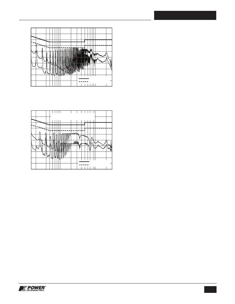
�Frequency� (MHz)�
�Figure� 45a.� Fixed� Frequency� Operation� Without� Jitter.�
�input� capacitor� negative� terminal� through� a� separate� trace� that�
�is� not� shared� by� the� components� connected� to� CONTROL,�
�MULTI-FUNCTION,� VOLTAGE� MONITOR� or� EXTERNAL�
�80�
�70�
�60�
�50�
�40�
�30�
�20�
�TOPSwitch-HX (with jitter)�
�CURRENT� LIMIT� pins.� This� is� because� the� SOURCE� pin� is� also�
�the� controller� ground� reference� pin.� Any� traces� to� the� M,� V,� X� or�
�C� pins� should� be� kept� as� short� as� possible� and� away� from� the�
�DRAIN� trace� to� prevent� noise� coupling.� VOLTAGE� MONITOR�
�resistors� (R1� and� R2� in� Figures� 46,� 47,� 48,� R3� and� R4� in�
�Figure� 49,� and� R14� in� Figure� 50)� should� be� located� close� to� the�
�M� or� V� pin� to� minimize� the� trace� length� on� the� M� or� V� pin� side.�
�Resistors� connected� to� the� M,� V� or� X� pin� should� be� connected�
�as� close� to� the� bulk� cap� positive� terminal� as� possible� while�
�routing� these� connections� away� from� the� power� switching�
�-10�
�0�
�-10�
�-20�
�0.15�
�1�
�EN55022B� (QP)�
�EN55022B� (AV)�
�10�
�30�
�circuitry.� In� addition� to� the� 47� μF� CONTROL� pin� capacitor,� a�
�high� frequency� bypass� capacitor� in� parallel� may� be� used� for�
�better� noise� immunity.� The� feedback� optocoupler� output�
�should� also� be� located� close� to� the� CONTROL� and� SOURCE�
�pins� of� TOPSwitch-HX� and� away� from� the� drain� and� clamp�
�component� traces.�
�Frequency� (MHz)�
�Figure� 45b.� TOPSwitch-HX� Full� Range� EMI� Scan� (132� kHz� With� Jitter)� With�
�Identical� Circuitry� and� Conditions.�
�Standby� Consumption�
�Frequency� reduction� can� significantly� reduce� power� loss� at� light�
�or� no� load,� especially� when� a� Zener� clamp� is� used.� For� very� low�
�secondary� power� consumption,� use� a� TL431� regulator� for�
�feedback� control.� A� typical� TOPSwitch-HX� circuit� automatically�
�enters� MCM� mode� at� no� load� and� the� low� frequency� mode� at�
�light� load,� which� results� in� extremely� low� losses� under� no-load�
�or� standby� conditions.�
�High� Power� Designs�
�The� TOPSwitch-HX� family� contains� parts� that� can� deliver� up� to�
�333� W.� High� power� designs� need� special� considerations.�
�Guidance� for� high� power� designs� can� be� found� in� the� Design�
�Guide� for� TOPSwitch-HX� (AN-43).�
�TOPSwitch-HX� Layout� Considerations�
�The� TOPSwitch-HX� has� multiple� pins� and� may� operate� at�
�Y� Capacitor�
�The� Y� capacitor� should� be� connected� close� to� the� secondary�
�output� return� pin(s)� and� the� positive� primary� DC� input� pin� of� the�
�transformer.�
�Heat� Sinking�
�The� tab� of� the� Y� package� (TO-220C)� and� E� package� (eSIP-7C)�
�and� L� package� (eSIP-7F)� are� internally� electrically� tied� to� the�
�SOURCE� pin.� To� avoid� circulating� currents,� a� heat� sink�
�attached� to� the� tab� should� not� be� electrically� tied� to� any� primary�
�ground/source� nodes� on� the� PC� board.� When� using� a� P� (DIP-8),�
�G� (SMD-8)� or� M� (DIP-10)� package,� a� copper� area� underneath�
�the� package� connected� to� the� SOURCE� pins� will� act� as� an�
�effective� heat� sink.� On� double� sided� boards,� topside� and� bottom�
�side� areas� connected� with� vias� can� be� used� to� increase� the�
�effective� heat� sinking� area.� In� addition,� sufficient� copper� area�
�should� be� provided� at� the� anode� and� cathode� leads� of� the�
�output� diode(s)� for� heat� sinking.� In� Figures� 46� to� 50� a� narrow�
�trace� is� shown� between� the� output� rectifier� and� output� filter�
�capacitor.� This� trace� acts� as� a� thermal� relief� between� the� rectifier�
�and� filter� capacitor� to� prevent� excessive� heating� of� the� capacitor.�
�high� power� levels.� The� following� guidelines� should� be�
�carefully� followed.�
�27�
�www.powerint.com�
�Rev.� H� 06/13�
�相关PDF资料 |
PDF描述 |
|---|---|
| TAJC156K010RNJ | CAP TANT 15UF 10V 10% 2312 |
| EEM03DRKN | CONN EDGECARD 6POS DIP .156 SLD |
| ABM43DSEF-S243 | CONN EDGECARD 86POS .156 EYELET |
| TAJC106K010H | CAP TANT 10UF 10V 10% 2312 |
| NLCV25T-R68M-PFR | INDUCTOR POWER .68UH 1008 |
相关代理商/技术参数 |
参数描述 |
|---|---|
| TOP256LG | 功能描述:交流/直流开关转换器 64W (85-264VAC) 88W (230V AC) RoHS:否 制造商:STMicroelectronics 输出电压:800 V 输入/电源电压(最大值):23.5 V 输入/电源电压(最小值):11.5 V 开关频率:115 kHz 电源电流:1.6 mA 工作温度范围:- 40 C to + 150 C 安装风格:SMD/SMT 封装 / 箱体:SSO-10 封装:Reel |
| TOP256LN | 功能描述:交流/直流开关转换器 64W (85-264VAC) 88W (230V AC) RoHS:否 制造商:STMicroelectronics 输出电压:800 V 输入/电源电压(最大值):23.5 V 输入/电源电压(最小值):11.5 V 开关频率:115 kHz 电源电流:1.6 mA 工作温度范围:- 40 C to + 150 C 安装风格:SMD/SMT 封装 / 箱体:SSO-10 封装:Reel |
| TOP256MG | 功能描述:交流/直流开关转换器 26W/40W PK 85-264VAC 34W/63W PK (230V AC) RoHS:否 制造商:STMicroelectronics 输出电压:800 V 输入/电源电压(最大值):23.5 V 输入/电源电压(最小值):11.5 V 开关频率:115 kHz 电源电流:1.6 mA 工作温度范围:- 40 C to + 150 C 安装风格:SMD/SMT 封装 / 箱体:SSO-10 封装:Reel |
| TOP256MN | 功能描述:交流/直流开关转换器 Off-Line Switcher IC 26W/64W PK RoHS:否 制造商:STMicroelectronics 输出电压:800 V 输入/电源电压(最大值):23.5 V 输入/电源电压(最小值):11.5 V 开关频率:115 kHz 电源电流:1.6 mA 工作温度范围:- 40 C to + 150 C 安装风格:SMD/SMT 封装 / 箱体:SSO-10 封装:Reel |
| TOP256PG | 功能描述:交流/直流开关转换器 26W/40W PK 85-264VAC 34W/63W PK (230V AC) RoHS:否 制造商:STMicroelectronics 输出电压:800 V 输入/电源电压(最大值):23.5 V 输入/电源电压(最小值):11.5 V 开关频率:115 kHz 电源电流:1.6 mA 工作温度范围:- 40 C to + 150 C 安装风格:SMD/SMT 封装 / 箱体:SSO-10 封装:Reel |
发布紧急采购,3分钟左右您将得到回复。