- 您现在的位置:买卖IC网 > PDF目录97770 > TPS3613-01DGST (TEXAS INSTRUMENTS INC) 1-CHANNEL POWER SUPPLY SUPPORT CKT, PDSO10 PDF资料下载
参数资料
| 型号: | TPS3613-01DGST |
| 厂商: | TEXAS INSTRUMENTS INC |
| 元件分类: | 电源管理 |
| 英文描述: | 1-CHANNEL POWER SUPPLY SUPPORT CKT, PDSO10 |
| 封装: | PLASTIC, MSOP-10 |
| 文件页数: | 6/10页 |
| 文件大小: | 142K |
| 代理商: | TPS3613-01DGST |
TPS3613-01
ADJUSTABLE BATTERY-BACKUP SUPERVISOR
FOR RAM RETENTION
SLVS340 – DECEMBER 2000
5
POST OFFICE BOX 655303
DALLAS, TEXAS 75265
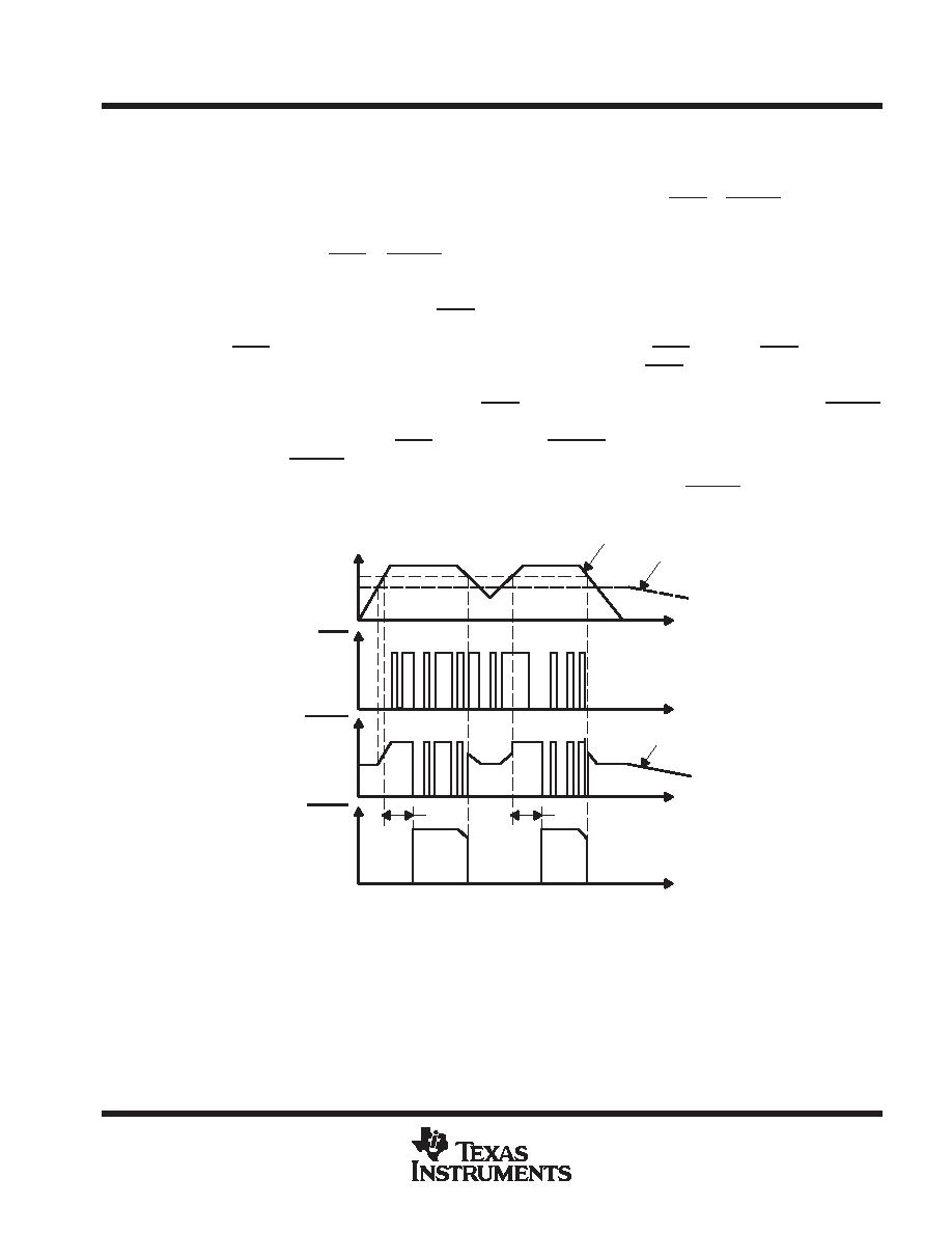
detailed description (continued)
chip-enable signal gating
The internal gating of chip-enable (CE) signals prevents erroneous data from corrupting CMOS RAM during
an under-voltage condition. The TPS3613 use a series transmission gate from CEIN to CEOUT. During normal
operation (reset not asserted), the CE transmission gate is enabled and passes all CE transitions. When reset
is asserted, this path becomes disabled, preventing erroneous data from corrupting the CMOS RAM. The short
CE propagation delay from CEIN to CEOUT enables the TPS3613 device to be used with most processors.
chip-enable signal gating (continued)
The CE transmission gate is disabled and CEIN is high impedance (disable mode) while reset is asserted.
During a power-down sequence when VDD crosses the reset threshold, the CE transmission gate will be
disabled and CEIN immediately becomes high impedance if the voltage at CEIN is high. If CEIN is low when
reset is asserted, the CE transmission gate will be disabled same time when CEIN goes high, or 10
s after reset
asserts, whichever occurs first. This will allow the current write cycle to complete during power down. When the
CE transmission gate is enabled, the impedance of CEIN appears as a resistor in series with the load at CEOUT.
The overall device propagation delay through the CE transmission gate depends on VOUT, the source
impedance of the drive connected to CEIN, and the load at CEOUT. To achieve minimum propagation delay,
the capacitive load at CEOUT should be minimized, and a low-output-impedance driver is used.
In the disabled mode, the transmission gate is off and an active pullup connects CEOUT to VOUT. This pullup
turns off when the transmission gate is enabled.
VIT
CEIN
CEOUT
RESET
td
t
VDD
VBAT
Figure 2. Chip-Enable Timing
相关PDF资料 |
PDF描述 |
|---|---|
| TPS658610ZQZT | 11-CHANNEL POWER SUPPLY MANAGEMENT CKT, PBGA120 |
| TPS658610ZQZR | 11-CHANNEL POWER SUPPLY MANAGEMENT CKT, PBGA120 |
| TPSCC6.5MB-TC10 | 2 SECTIONS - 2 SECTIONS, 6.5 MHz, CERAMIC BRF |
| TPSCC6.0MB-TC10 | 2 SECTIONS - 2 SECTIONS, 6 MHz, CERAMIC BRF |
| TPSCC5.5MB-TC10 | 2 SECTIONS - 2 SECTIONS, 5.5 MHz, CERAMIC BRF |
相关代理商/技术参数 |
参数描述 |
|---|---|
| TPS3613-18DGSR | 制造商:未知厂家 制造商全称:未知厂家 功能描述:Analog IC |
| TPS3613-18DGST | 制造商:未知厂家 制造商全称:未知厂家 功能描述:Analog IC |
| TPS3613-25DGSR | 制造商:未知厂家 制造商全称:未知厂家 功能描述:Analog IC |
| TPS3613-25DGST | 制造商:未知厂家 制造商全称:未知厂家 功能描述:Analog IC |
| TPS3613-30DGSR | 制造商:未知厂家 制造商全称:未知厂家 功能描述:Analog IC |
发布紧急采购,3分钟左右您将得到回复。