- 您现在的位置:买卖IC网 > PDF目录98281 > TPS40074RHL (TEXAS INSTRUMENTS INC) 2 A SWITCHING CONTROLLER, 550 kHz SWITCHING FREQ-MAX, PQCC20 PDF资料下载
参数资料
| 型号: | TPS40074RHL |
| 厂商: | TEXAS INSTRUMENTS INC |
| 元件分类: | 稳压器 |
| 英文描述: | 2 A SWITCHING CONTROLLER, 550 kHz SWITCHING FREQ-MAX, PQCC20 |
| 封装: | PLASTIC, QFN-20 |
| 文件页数: | 34/37页 |
| 文件大小: | 448K |
| 代理商: | TPS40074RHL |
第1页第2页第3页第4页第5页第6页第7页第8页第9页第10页第11页第12页第13页第14页第15页第16页第17页第18页第19页第20页第21页第22页第23页第24页第25页第26页第27页第28页第29页第30页第31页第32页第33页当前第34页第35页第36页第37页
www.ti.com
TPS40074
SLUS617–APRIL 2005
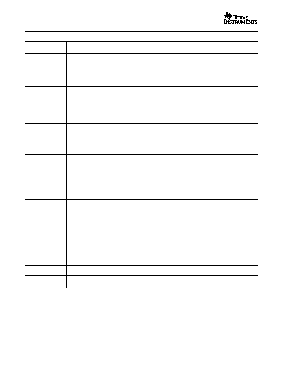
Table 1. TERMINAL FUNCTIONS
TERMINAL
I/O
DESCRIPTION
NAME
NO.
The BOOST voltage is 8-V greater than the input voltage. The peak voltage on BOOST is equal to the SW node
voltage plus the voltage present at DBP less the bootstrap diode drop. This drop can be 1.4 V for the internal
BOOST
11
I
bootstrap diode or 300 mV for an external schottkey diode. The voltage differential between this pin and SW is the
available drive voltage for the high-side FET.
Output of the error amplifier, input to the PWM comparator. A feedback network is connected from this pin to the
COMP
6
O
FB pin to compensate the overall loop. This pin is internally clamped to a 3.4-V maximum output drive capability
for quicker recovery from a saturated feedback loop situation.
8-V regulator output used for the gate drive of the N-channel synchronous rectifier and as the supply for charging
DBP
9
O
the bootstrap capacitor. This pin should be bypassed to ground with a 1.0-F ceramic capacitor.
Inverting input to the error amplifier. In normal operation the voltage on this pin is equal to the internal reference
FB
5
I
voltage, 0.7 V.
GND
3
-
Ground reference for the device.
Floating gate drive for the high-side N-channel MOSFET. This pin switches from BOOST (MOSFET on) to SW
HDRV
12
O
(MOSFET off).
Short circuit protection programming pin. This pin is used to set the overcurrent threshold. An internal current sink
from this pin to ground sets a voltage drop across an external resistor connected from this pin to VDD. The voltage
on this pin is compared to the voltage drop (VVDD -VSW) across the high side N-channel MOSFET during
ILIM
14
I
conduction. Just prior to the beginning of a switching cycle this pin is pulled to approximately VVDD/2 and released
when SW is within 2 V of VVDD or after a timeout (the precondition time) - whichever occurs first. Placing a
capacitor across the resistor from ILIM to VDD allows the ILIM threshold to decrease during the switch on time,
effectively programming the ILIM blanking time. See Applications Information section.
A resistor is connected from this pin to VDD programs the amount of input voltage feed-forward. The current fed
KFF
15
I
into this pin is used to control the slope of the PWM ramp and program undervoltage lockout. Nominal voltage at
this pin is maintained at 400 mV.
Gate drive for the N-channel synchronous rectifier. This pin switches from DBP (MOSFET on) to PGND (MOSFET
LDRV
8
O
off).
4.2-V reference used for internal device logic and analog functions. This pin should be bypassed to GND with a
LVBP
17
O
0.1-F ceramic capacitor. External loads less than 1 mA and electrically quiet may be applied.
This is an open drain output that pulls to ground when soft start is active, or when the FB pin is outside a ±10%
PGD
18
O
band around the 700 mV reference voltage.
Power ground reference for the device. There should be a low-impedance path from this pin to the source(s) of the
PGND
7
lower MOSFET(s).
RT
16
I
A resistor is connected from this pin to GND to set the switching frequency.
SA+
20
I
Noninverting input of the remote voltage sense amplifier.
SA-
1
I
Inverting input of the remote voltage sense amplifier.
SAO
2
O
Output of the remote voltage sense amplifier.
Soft-start programming pin. A capacitor connected from this pin to GND programs the soft-start time. The
capacitor is charged with an internal current source of 12 A. The resulting voltage ramp on the SS pin is used as
a second non-inverting input to the error amplifier. The voltage at this error amplifier input is approximately 1 V
SS
4
I
less that that on the SS pin. Output voltage regulation is controlled by the SS voltage ramp until the voltage on the
SS pin reaches the internal offset voltage of 1 V plus the internal reference voltage of 700 mV. If SS is below the
internal offset voltage of 1 V (300 mV minimum ensured), the resulting output voltage is zero. Also provides timing
for fault recovery attempts.
This pin is connected to the switched node of the converter and used for overcurrent sensing as well as gate drive
SW
10
I
timing. This pin is also the return path from the high-side FET for the floating high-side FET driver.
SYNC
19
I
Logic input for pulse train to synchronize oscillator.
VDD
13
I
Supply voltage for the device.
6
相关PDF资料 |
PDF描述 |
|---|---|
| TPS40075RHLR | 2 A SWITCHING CONTROLLER, 1000 kHz SWITCHING FREQ-MAX, PQCC20 |
| TPS40075RHLTG4 | 2 A SWITCHING CONTROLLER, 1000 kHz SWITCHING FREQ-MAX, PQCC20 |
| TPS40077PWPR | 2 A SWITCHING CONTROLLER, 1000 kHz SWITCHING FREQ-MAX, PDSO16 |
| TPS40077PWPRG4 | 2 A SWITCHING CONTROLLER, 1000 kHz SWITCHING FREQ-MAX, PDSO16 |
| TPS40077PWPG4 | 2 A SWITCHING CONTROLLER, 1000 kHz SWITCHING FREQ-MAX, PDSO16 |
相关代理商/技术参数 |
参数描述 |
|---|---|
| TPS40074RHLR | 功能描述:DC/DC 开关控制器 Mid Input Sync Buck w/Vltg Feed-Fwd RoHS:否 制造商:Texas Instruments 输入电压:6 V to 100 V 开关频率: 输出电压:1.215 V to 80 V 输出电流:3.5 A 输出端数量:1 最大工作温度:+ 125 C 安装风格: 封装 / 箱体:CPAK |
| TPS40074RHLRG4 | 功能描述:DC/DC 开关控制器 Mid Input Sync Buck w/Vltg Feed-Fwd RoHS:否 制造商:Texas Instruments 输入电压:6 V to 100 V 开关频率: 输出电压:1.215 V to 80 V 输出电流:3.5 A 输出端数量:1 最大工作温度:+ 125 C 安装风格: 封装 / 箱体:CPAK |
| TPS40074RHLT | 功能描述:DC/DC 开关控制器 Mid Input Sync Buck w/Vltg Feed-Fwd RoHS:否 制造商:Texas Instruments 输入电压:6 V to 100 V 开关频率: 输出电压:1.215 V to 80 V 输出电流:3.5 A 输出端数量:1 最大工作温度:+ 125 C 安装风格: 封装 / 箱体:CPAK |
| TPS40074RHLTG4 | 功能描述:DC/DC 开关控制器 Mid Input Sync Buck w/Vltg Feed-Fwd RoHS:否 制造商:Texas Instruments 输入电压:6 V to 100 V 开关频率: 输出电压:1.215 V to 80 V 输出电流:3.5 A 输出端数量:1 最大工作温度:+ 125 C 安装风格: 封装 / 箱体:CPAK |
| TPS40075 | 制造商:TI 制造商全称:Texas Instruments 功能描述:4.5V TO 18V INPUT 10 PIN SYNCHRONOUS BUCK CONTROLLER WITH POWER GOOD |
发布紧急采购,3分钟左右您将得到回复。