- 您现在的位置:买卖IC网 > PDF目录69509 > TPS40130RHBR (TEXAS INSTRUMENTS INC) SWITCHING CONTROLLER, 1200 kHz SWITCHING FREQ-MAX, PQCC32 PDF资料下载
参数资料
| 型号: | TPS40130RHBR |
| 厂商: | TEXAS INSTRUMENTS INC |
| 元件分类: | 稳压器 |
| 英文描述: | SWITCHING CONTROLLER, 1200 kHz SWITCHING FREQ-MAX, PQCC32 |
| 封装: | GREEN, PLASTIC, QFN-32 |
| 文件页数: | 37/38页 |
| 文件大小: | 950K |
| 代理商: | TPS40130RHBR |
第1页第2页第3页第4页第5页第6页第7页第8页第9页第10页第11页第12页第13页第14页第15页第16页第17页第18页第19页第20页第21页第22页第23页第24页第25页第26页第27页第28页第29页第30页第31页第32页第33页第34页第35页第36页当前第37页第38页
www.ti.com
SLUS602B – JUNE 2004 – REVISED SEPTEMBER 2005
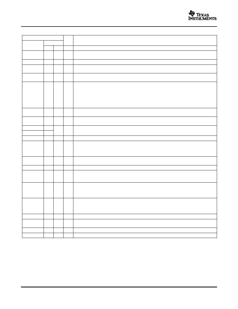
Terminal Functions (continued)
TERMINAL
I/O
DESCRIPTION
NO.
NAME
RHB
DBT
Inverting input of the error amplifier. In closed loop operation, the voltage at this pin is the internal
FB
12
15
I
reference level of 700 mV. This pin is also used for the PGOOD and undervoltage comparators.
GSNS
4
8
I
Inverting input of the differential amplifier. This pin should be connected to ground at the point of load.
Gate drive output for the high-side N-channel MOSFET switch for PWM1. Output is referenced to
HDRV1
32
4
O
SW1 and is bootstrapped for enhancement of the high-side switch.
Gate drive output for the high-side N-channel MOSFET switch for PWM2. Output is referenced to
HDRV2
25
27
O
SW2 and is bootstrapped for enhancement of the high-side switch
Used to set the cycle-by-cycle current limit threshold. If ILIM threshold is reached, the PWM cycle is
terminated and the converter delivers limited current to the output. Under these conditions the
undervoltage threshold eventually is reached and the controller enters the hiccup mode. The
ILIM
14
17
I
controller stays in the hiccup mode for seven (7) consecutive cycles of SS voltage rising from zero to
1.0 V. At the eighth cycle the controller attempts a full start-up sequence. The relationship between
ILIM and the maximum phase current is described in Equation 4 and Equation 5. See the Overcurrent
Protection section for more details.
Gate drive output for the low-side synchronous rectifier (SR) N-channel MOSFET for PWM1. See
LDRV1
29
1
O
Layout Considerations section.
Gate drive output for the low-side synchronous rectifier (SR) N-channel MOSFET for PWM2. See
LDRV2
27
29
O
Layout Considerations section.
NC
8
-
No connect. This pin is mechanical only.
NC
24
OVSET
2
6
I
A resistor divider, on this pin connected to the output voltage sets the overvoltage sense point.
Power good indicator of the output voltage. This open-drain output connects to a voltage via an
external resistor. When the FB pin voltage is between 0.616 V to 0.784 V (88% to 112% of VREF),
PGOOD
15
18
O
the PGOOD output is in a high impedance state. If the DROOP function is implemented, the
programmed droop voltage must be within this window.
Power ground reference for the controller lower gate drivers. There should be a high-current return
PGND
28
30
-
path from the sources of the lower MOSFETs to this pin.
RT
16
19
I
Connecting a resistor from this pin to ground sets the oscillator frequency.
Provides user programmable soft-start by means of a capacitor connected to the pin. If an
SS
22
25
I
undervoltage fault is detected the soft-start capacitor cycles 7 times with no switching before a normal
soft-start sequence allowed.
Connect to the switched node on converter 1. Power return for the channel 1 upper gate driver. There
should be a high-current return path from the source of the upper MOSFET to this pin. It is also used
SW1
31
3
I
by the adaptive gate drive circuits to minimize the dead time between upper and lower MOSFET
conduction.
Connect to the switched node on converter 2. Power return for the channel 2 upper gate driver. There
should be a high-current return path from the source of the upper MOSFET to this pin. It is also used
SW2
26
28
I
by the adaptive gate drive circuits to minimize the dead time between upper and lower MOSFET
conduction.
UVLO
21
24
O
A voltage divider from VIN to this pin, set to 1V, determines the input voltage that starts the controller.
Non-inverting input of the differential amplifier. This pin should be connected to VOUT at the point of
VOUT
3
7
O
load.
VREF
10
13
O
Output of an internal reference voltage. The load may be up to 100 A DC.
VIN5
30
2
I
Power input for the device. A 1.0-F ceramic capacitor should be connected from this pin to ground.
8
相关PDF资料 |
PDF描述 |
|---|---|
| TPS40130RHBRG4 | SWITCHING CONTROLLER, 1200 kHz SWITCHING FREQ-MAX, PQCC32 |
| TPS40130RHB | SWITCHING CONTROLLER, 1200 kHz SWITCHING FREQ-MAX, PQCC32 |
| TPS40140RHHTG4 | 0.1 A DUAL SWITCHING CONTROLLER, 1000 kHz SWITCHING FREQ-MAX, PQCC36 |
| TPS40140RHHT | 0.1 A DUAL SWITCHING CONTROLLER, 1000 kHz SWITCHING FREQ-MAX, PQCC36 |
| TPS40140RHHR | 0.1 A DUAL SWITCHING CONTROLLER, 1000 kHz SWITCHING FREQ-MAX, PQCC36 |
相关代理商/技术参数 |
参数描述 |
|---|---|
| TPS40130RHBRG4 | 功能描述:DC/DC 开关控制器 2-Ch Multiphase Buck DC/DC w/Int Drvr RoHS:否 制造商:Texas Instruments 输入电压:6 V to 100 V 开关频率: 输出电压:1.215 V to 80 V 输出电流:3.5 A 输出端数量:1 最大工作温度:+ 125 C 安装风格: 封装 / 箱体:CPAK |
| TPS40130RHBT | 功能描述:DC/DC 开关控制器 2-Ch Multiphase Buck DC/DC w/Int Drvr RoHS:否 制造商:Texas Instruments 输入电压:6 V to 100 V 开关频率: 输出电压:1.215 V to 80 V 输出电流:3.5 A 输出端数量:1 最大工作温度:+ 125 C 安装风格: 封装 / 箱体:CPAK |
| TPS40130RHBTG4 | 功能描述:DC/DC 开关控制器 2-Ch Multiphase Buck DC/DC w/Int Drvr RoHS:否 制造商:Texas Instruments 输入电压:6 V to 100 V 开关频率: 输出电压:1.215 V to 80 V 输出电流:3.5 A 输出端数量:1 最大工作温度:+ 125 C 安装风格: 封装 / 箱体:CPAK |
| TPS40131 | 制造商:TI 制造商全称:Texas Instruments 功能描述:TWO-PHASE, SYNCHRONOUS BUCK CONTROLLER WITH INTEGRATED MOSFET DRIVERS |
| TPS40131EVM | 功能描述:电源管理IC开发工具 TPS40131 Eval Mod RoHS:否 制造商:Maxim Integrated 产品:Evaluation Kits 类型:Battery Management 工具用于评估:MAX17710GB 输入电压: 输出电压:1.8 V |
发布紧急采购,3分钟左右您将得到回复。