- 您现在的位置:买卖IC网 > PDF目录98285 > TPS65055RSMR (TEXAS INSTRUMENTS INC) 1.8 A DUAL SWITCHING CONTROLLER, 2475 kHz SWITCHING FREQ-MAX, PQCC32 PDF资料下载
参数资料
| 型号: | TPS65055RSMR |
| 厂商: | TEXAS INSTRUMENTS INC |
| 元件分类: | 稳压器 |
| 英文描述: | 1.8 A DUAL SWITCHING CONTROLLER, 2475 kHz SWITCHING FREQ-MAX, PQCC32 |
| 封装: | 4 X 4 MM, GREEN, PLASTIC, QFN-32 |
| 文件页数: | 14/41页 |
| 文件大小: | 1276K |
| 代理商: | TPS65055RSMR |
第1页第2页第3页第4页第5页第6页第7页第8页第9页第10页第11页第12页第13页当前第14页第15页第16页第17页第18页第19页第20页第21页第22页第23页第24页第25页第26页第27页第28页第29页第30页第31页第32页第33页第34页第35页第36页第37页第38页第39页第40页第41页
THERMAL SHUTDOWN
LDO1 to LDO4
Default Voltage Setting for LDOs and DCDC1
INTERFACE SPECIFICATION
Serial Interface
www.ti.com.......................................................................................................................................................................................... SLVS844 – SEPTEMBER 2008
As soon as the junction temperature, TJ, exceeds typically 150°C for the dcdc converters, the device goes into
thermal shutdown. In this mode, the P- and N-Channel MOSFETs are turned-off. The device continues its
operation when the junction temperature falls below the thermal shutdown hysteresis again. A thermal shutdown
for one of the dcdc converters disables both converters simultaneously.
The thermal shutdown temperature for the LDOs are set to typically 140°C. Therefore, a LDO which may be
used to power an external voltage never heats up the device that high to turn off the dcdc converters. If one LDO
exceeds the thermal shutdown temperature, all LDOs turn off simultaneously.
The low dropout voltage regulators are designed to operate well with low value ceramic input and output
capacitors. They operate with input voltages down to 1.5 V. The LDOs offer a maximum dropout voltage of 280
mV at rated output current. Each LDO supports a current limit feature. The LDOs are enabled by the EN_LDO1,
ENLDO2, EN_LDO3, and EN_LDO4 pin EXOR with a bit in register REG_CTRL (Reg#02h).
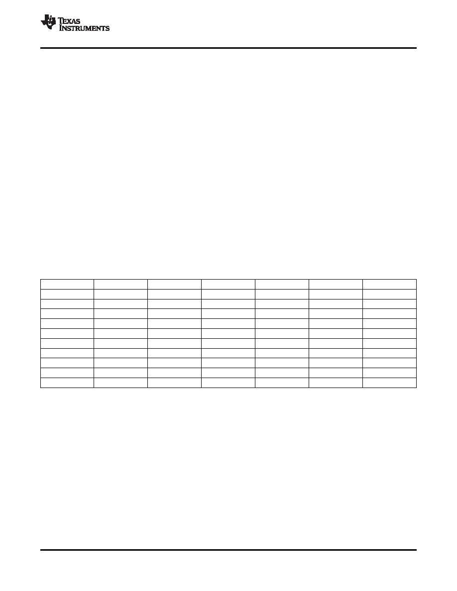
In the TPS65055, the output voltage of the LDOs and of DCDC1 is set using two pins, DEFLDO1 and DEFLDO2.
These pins can either be connected to a logic low level, a logic high level, or left floating to define a set of output
voltages for LDO1 to LDO4 and DCDC1 according to the following table. The status of the DEFLDO pins is
latched after an undervoltage lockout event (UVLO) and sets the registers LDO_CTRL1, LDO_CTRL2, and
DEFDCDC1 accordingly. The output voltage of each LDO and DCDC1 can be changed later by reprogramming
these registers. See the register description for more details.
The TPS65055 default voltage options are adjustable with DEFLDO2 and DEFLDO1 according to the following
table:
DEFLDO2
DEFLDO1
VLDO1
VLDO2
VLDO3
VLDO4
DCDC1
400mA LDO
200mA LDO
600mA
0
1.2 V
1.8 V
2.8 V
1.3 V
2.1 V
0
float
1.2 V
1.8 V
2.8 V
1.8 V
0
1
1.2 V
1.8 V
2.8 V
1.3 V
1.8 V
float
0
1.2 V
1.8 V
2.8 V
2.1 V
float
1.2 V
1.8 V
2.8 V
1.8 V
2.1 V
float
1
1.2 V
1.8 V
2.8 V
1.2 V
1
0
1.2 V
1.8 V
2.8 V
1.0 V
1.9 V
1
float
1.2 V
1.8 V
2.8 V
3.0 V
2.1 V
1
1.0 V
1.2 V
1.0 V
1.2 V
The serial interface is compatible with the standard and fast mode I2C specifications, allowing transfers at up to
400 kHz. The interface adds flexibility to the power supply solution, enabling most functions to be programmed to
new values depending on the instantaneous application requirements and charger status to be monitored.
Register contents remain intact as long as VCC remains above the UVLO threshold. The TPS65055 has a 7bit
address: ‘1001000’, other addresses are available upon contact with the factory. Attempting to read data from
register addresses not listed in this section result in 00h being read out.
For normal data transfer, DATA is allowed to change only when CLK is low. Changes when CLK is high are
reserved for indicating the start and stop conditions. During data transfer, the data line must remain stable
whenever the clock line is high. There is one clock pulse per bit of data. Each data transfer is initiated with a start
condition and terminated with a stop condition. When addressed, the TPS65055 device generates an
acknowledge bit after the reception of each byte. The master device (microprocessor) must generate an extra
clock pulse that is associated with the acknowledge bit. The TPS65055 device must pull down the DATA line
during the acknowledge clock pulse so that the DATA line is a stable low during the high period of the
Copyright 2008, Texas Instruments Incorporated
21
Product Folder Link(s): TPS65055
相关PDF资料 |
PDF描述 |
|---|---|
| TPS65058RGET | 1.8 A DUAL SWITCHING CONTROLLER, 2475 kHz SWITCHING FREQ-MAX, PQCC32 |
| TPS650732TRSLRQ1 | POWER SUPPLY SUPPORT CKT, PQCC48 |
| TPS65110RGEG3 | SWITCHED CAPACITOR REGULATOR, 520 kHz SWITCHING FREQ-MAX, PQCC24 |
| TPS65130RGER | 0.9 A SWITCHING REGULATOR, 1500 kHz SWITCHING FREQ-MAX, PQCC24 |
| TPS65130RGET | 0.9 A SWITCHING REGULATOR, 1500 kHz SWITCHING FREQ-MAX, PQCC24 |
相关代理商/技术参数 |
参数描述 |
|---|---|
| TPS65055RSMRG4 | 功能描述:PMIC 解决方案 Dual buck w/ 4LDO & I2C RoHS:否 制造商:Texas Instruments 安装风格:SMD/SMT 封装 / 箱体:QFN-24 封装:Reel |
| TPS65055RSMT | 功能描述:PMIC 解决方案 Dual buck w/ 4LDO & I2C RoHS:否 制造商:Texas Instruments 安装风格:SMD/SMT 封装 / 箱体:QFN-24 封装:Reel |
| TPS65055RSMTG4 | 功能描述:PMIC 解决方案 Dual buck w/ 4LDO & I2C RoHS:否 制造商:Texas Instruments 安装风格:SMD/SMT 封装 / 箱体:QFN-24 封装:Reel |
| TPS65056EVM-195 | 功能描述:电源管理IC开发工具 TPS65056 Eval Mod RoHS:否 制造商:Maxim Integrated 产品:Evaluation Kits 类型:Battery Management 工具用于评估:MAX17710GB 输入电压: 输出电压:1.8 V |
| TPS65056RSMR | 功能描述:PMIC 解决方案 6Ch Pwr Mgmt IC RoHS:否 制造商:Texas Instruments 安装风格:SMD/SMT 封装 / 箱体:QFN-24 封装:Reel |
发布紧急采购,3分钟左右您将得到回复。