- 您现在的位置:买卖IC网 > PDF目录69523 > TPS84320RUQT (TEXAS INSTRUMENTS INC) 3 A SWITCHING REGULATOR, 390 kHz SWITCHING FREQ-MAX, PQCC47 PDF资料下载
参数资料
| 型号: | TPS84320RUQT |
| 厂商: | TEXAS INSTRUMENTS INC |
| 元件分类: | 稳压器 |
| 英文描述: | 3 A SWITCHING REGULATOR, 390 kHz SWITCHING FREQ-MAX, PQCC47 |
| 封装: | 9 X 15 MM, 2.80 MM HEIGHT, GREEN, PLASTIC, QFN-47 |
| 文件页数: | 23/28页 |
| 文件大小: | 903K |
| 代理商: | TPS84320RUQT |
第1页第2页第3页第4页第5页第6页第7页第8页第9页第10页第11页第12页第13页第14页第15页第16页第17页第18页第19页第20页第21页第22页当前第23页第24页第25页第26页第27页第28页
SLUSAH7
– SEPTEMBER 2011
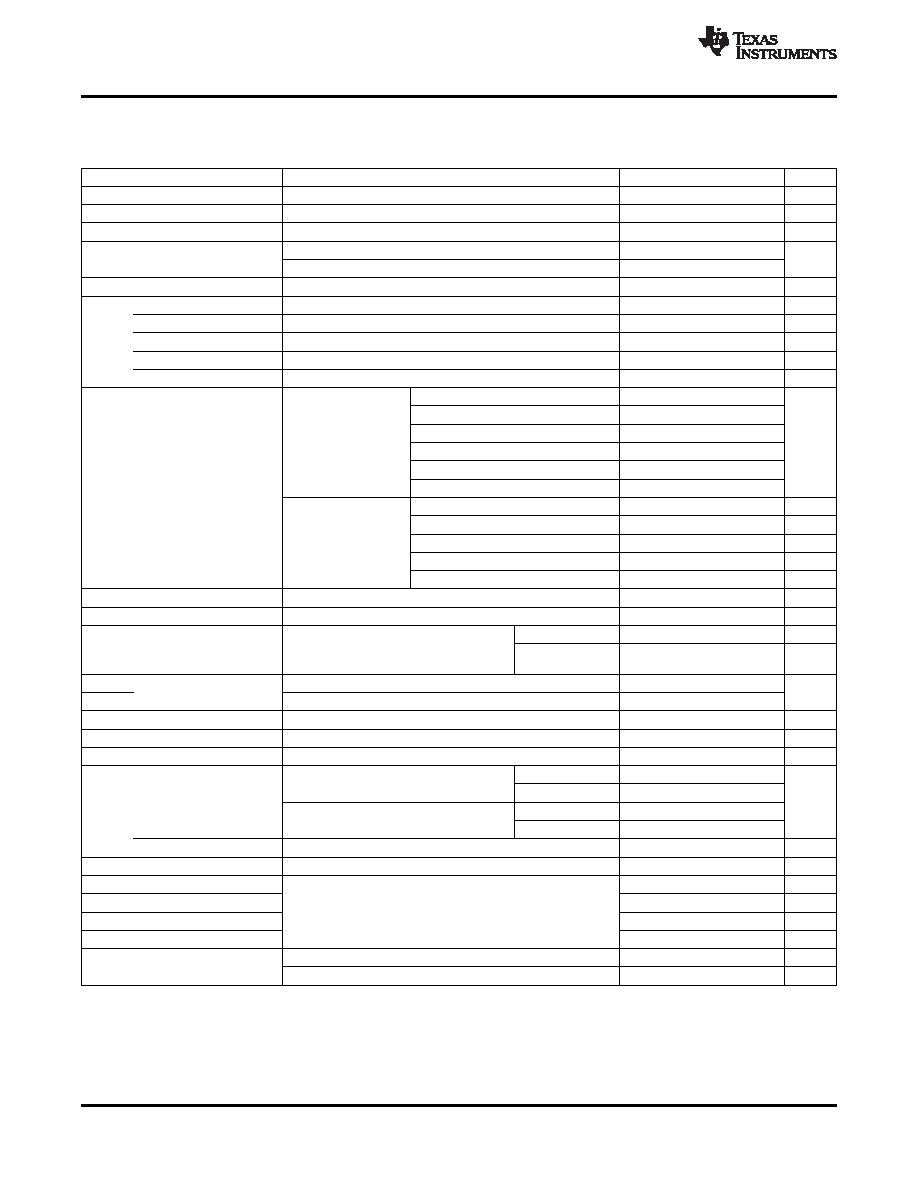
ELECTRICAL CHARACTERISTICS
Over -40
°C to 85°C free-air temperature, PVIN = VIN = 12 V, VOUT = 1.8 V, IOUT = 3A,
CIN1 = 2x 22 F ceramic, CIN2 = 68 F poly-tantalum, COUT1 = 4x 47 F ceramic (unless otherwise noted)
PARAMETER
TEST CONDITIONS
MIN
TYP
MAX
UNIT
IOUT
Output current
TA = 85°C, natural convection
0
3
A
VIN
Input bias voltage range
Over IOUT range
4.5
14.5
V
PVIN
Input switching voltage range
Over IOUT range
1.6(1)
14.5
V
VIN = increasing
4.0
4.5
UVLO
VIN Undervoltage lockout
V
VIN = decreasing
3.5
3.85
VOUT(adj)
Output voltage adjust range
Over IOUT range
0.8
5.5
V
Set-point voltage tolerance
TA = 25°C, IOUT = 0A
±1.0% (2)
Temperature variation
-40
°C ≤ TA ≤ +85°C, IOUT = 0A
±0.3%
VOUT
Line regulation
Over PVIN range, TA = 25°C, IOUT = 0A
±0.1%
Load regulation
Over IOUT range, TA = 25°C
±0.1%
Total output voltage variation
Includes set-point, line, load, and temperature variation
±1.5% (2)
VOUT = 5V, fSW = 780kHz
91.5 %
VOUT = 3.3V, fSW = 630kHz
89.0 %
VOUT = 2.5V, fSW = 480kHz
86.9 %
PVIN = VIN = 12 V
IO = 1.5 A
VOUT = 1.8V, fSW = 480kHz
85.2 %
VOUT = 1.2V, fSW = 480kHz
82.1 %
η
Efficiency
VOUT = 0.8V, fSW = 330kHz
78.7 %
PVIN = VIN = 5 V
VOUT = 3.3V, fSW = 630kHz
93.3 %
IO = 1.5 A
VOUT = 2.5V, fSW = 480kHz
91.4 %
VOUT = 1.8V, fSW = 480kHz
88.8 %
VOUT = 1.2V, fSW = 480kHz
85.2 %
VOUT = 0.8V, fSW = 330kHz
81.8 %
Output voltage ripple
20 MHz bandwith
35
mVPP
ILIM
Overcurrent threshold
5.8
A
Recovery time
190
s
Transient response
1.0 A/
s load step from 50 to 100% IOUT(max)
VOUT
35
mV
over/undershoot
VINH-H
Inhibit High Voltage
1.30
Open (3)
Inhibit Control
V
VINH-L
Inhibit Low Voltage
–0.3
1.05
INH Input current
INH
< 1.1 V
-1.15
μA
INH Hysteresis current
INH
> 1.26 V
-3.4
μA
II(stby)
Input standby current
INH pin to AGND
2
4
A
Good
94%
VOUT rising
Fault
109%
PWRGD Thresholds
Power
Fault
91%
Good
VOUT falling
Good
106%
PWRGD Low Voltage
I(PWRGD) = 2 mA
0.3
V
fSW
Switching frequency
Over VIN and IOUT ranges, RT/CLK pin OPEN
270
330
390
kHz
fCLK
Synchronization frequency
330
780
kHz
VCLK-H
CLK High-Level Threshold
2.0
5.5
V
CLK Control
VCLK-L
CLK Low-Level Threshold
0.8
V
DCLK
CLK Duty cycle
20%
80%
Thermal shutdown
160
175
°C
Thermal Shutdown
Thermal shutdown hysteresis
10
°C
(1)
The minimum PVIN voltage is 1.6V or (VOUT+ 0.7V) , whichever is greater. VIN must be greater than 4.5V.
(2)
The stated limit of the set-point voltage tolerance includes the tolerance of both the internal voltage reference and the internal
adjustment resistor. The overall output voltage tolerance will be affected by the tolerance of the external RSET resistor.
(3)
This control pin has an internal pullup. If this pin is left open circuit, the device operates when input power is applied. A small
low-leakage (
<300 nA) MOSFET is recommended for control. See the application section for further guidance.
4
Copyright
2011, Texas Instruments Incorporated
相关PDF资料 |
PDF描述 |
|---|---|
| TPS84410RKGT | 4 A SWITCHING REGULATOR, 600 kHz SWITCHING FREQ-MAX, PQCC39 |
| TPS84410RKGR | 4 A SWITCHING REGULATOR, 600 kHz SWITCHING FREQ-MAX, PQCC39 |
| TQN25A48S12 | 1-OUTPUT 300 W DC-DC REG PWR SUPPLY MODULE |
| TQN25A48S12 | 1-OUTPUT 300 W DC-DC REG PWR SUPPLY MODULE |
| TQN20A48S12 | 1-OUTPUT 240 W DC-DC REG PWR SUPPLY MODULE |
相关代理商/技术参数 |
参数描述 |
|---|---|
| TPS843F | 制造商:TOSHIBA 制造商全称:Toshiba Semiconductor 功能描述:Silicon Epitaxial Planar |
| TPS844 | 制造商:TOSHIBA 制造商全称:Toshiba Semiconductor 功能描述:Silicon Epitaxial Planar |
| TPS844(F) | 制造商:Toshiba America Electronic Components 功能描述: |
| TPS84410 | 制造商:TI 制造商全称:Texas Instruments 功能描述:2.95-V to 6-V Input, 4-A Synchronous Buck, Integrated Power Solution |
| TPS84410EVM-001 | 功能描述:电源管理IC开发工具 TPS84410 EVAL MOD RoHS:否 制造商:Maxim Integrated 产品:Evaluation Kits 类型:Battery Management 工具用于评估:MAX17710GB 输入电压: 输出电压:1.8 V |
发布紧急采购,3分钟左右您将得到回复。