- 您现在的位置:买卖IC网 > PDF目录69523 > TPS84320RUQT (TEXAS INSTRUMENTS INC) 3 A SWITCHING REGULATOR, 390 kHz SWITCHING FREQ-MAX, PQCC47 PDF资料下载
参数资料
| 型号: | TPS84320RUQT |
| 厂商: | TEXAS INSTRUMENTS INC |
| 元件分类: | 稳压器 |
| 英文描述: | 3 A SWITCHING REGULATOR, 390 kHz SWITCHING FREQ-MAX, PQCC47 |
| 封装: | 9 X 15 MM, 2.80 MM HEIGHT, GREEN, PLASTIC, QFN-47 |
| 文件页数: | 25/28页 |
| 文件大小: | 903K |
| 代理商: | TPS84320RUQT |
第1页第2页第3页第4页第5页第6页第7页第8页第9页第10页第11页第12页第13页第14页第15页第16页第17页第18页第19页第20页第21页第22页第23页第24页当前第25页第26页第27页第28页
SLUSAH7
– SEPTEMBER 2011
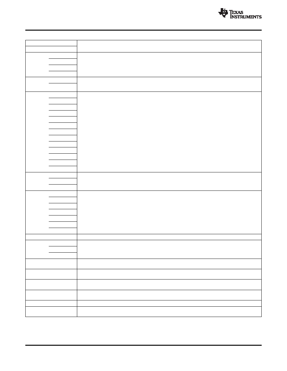
PIN DESCRIPTIONS
TERMINAL
DESCRIPTION
NAME
NO.
1
2
Zero VDC reference for the analog control circuitry. Connect AGND to PGND at a single point. Connect near
AGND
the output capacitors. See Figure 43 for a recommended layout.
34
45
8
Inhibit and UVLO adjust pin. Use an open drain or open collector output logic to control the INH function. A
INH/UVLO
resistor divider between this pin, AGND and VIN adjusts the UVLO voltage. Tie both pins together when
9
using this control.
3
4
5
15
16
18
Do Not Connect. Do not connect these pins to AGND, to another DNC pin, or to any other voltage. These
DNC
19
pins are connected to internal circuitry. Each pin must be soldered to an isolated pad.
20
22
23
30
31
32
36
Common ground connection for the PVIN, VIN, and VOUT power connections. See Figure 43 for a
PGND
37
recommended layout.
38
10
11
12
Phase switch node. These pins should be connected to a small copper island under the device for thermal
PH
13
relief. Do not place any external component on this pin or tie it to a pin of another function.
14
17
46
PWRGD
33
Power good fault pin. Asserts low if the output voltage is low. A pull-up resistor is required.
39
Input switching voltage. This pin supplies voltage to the power switches of the converter. See Figure 43 for a
PVIN
40
recommended layout.
41
This pin automatically selects between RT mode and CLK mode. An external timing resistor adjusts the
RT/CLK
35
switching frequency of the device. In CLK mode, the device synchronizes to an external clock.
Remote sense connection. Connect this pin to VOUT at the load for improved regulation. This pin must be
SENSE+
44
connected to VOUT at the load, or at the module pins.
Slow-start and tracking pin. Connecting an external capacitor to this pin adjusts the output voltage rise time.
SS/TR
6
A voltage applied to this pin allows for tracking and sequencing control.
Slow-start or track feature select. Connect this pin to AGND to enable the internal SS capacitor with a SS
STSEL
7
interval of approximately 1.1 ms. Leave this pin open to enable the TR feature.
VADJ
43
Connecting a resistor between this pin and AGND sets the output voltage.
Input bias voltage pin. Supplies the control circuitry of the power converter. See Figure 43 for a
VIN
42
recommended layout.
6
Copyright
2011, Texas Instruments Incorporated
相关PDF资料 |
PDF描述 |
|---|---|
| TPS84410RKGT | 4 A SWITCHING REGULATOR, 600 kHz SWITCHING FREQ-MAX, PQCC39 |
| TPS84410RKGR | 4 A SWITCHING REGULATOR, 600 kHz SWITCHING FREQ-MAX, PQCC39 |
| TQN25A48S12 | 1-OUTPUT 300 W DC-DC REG PWR SUPPLY MODULE |
| TQN25A48S12 | 1-OUTPUT 300 W DC-DC REG PWR SUPPLY MODULE |
| TQN20A48S12 | 1-OUTPUT 240 W DC-DC REG PWR SUPPLY MODULE |
相关代理商/技术参数 |
参数描述 |
|---|---|
| TPS843F | 制造商:TOSHIBA 制造商全称:Toshiba Semiconductor 功能描述:Silicon Epitaxial Planar |
| TPS844 | 制造商:TOSHIBA 制造商全称:Toshiba Semiconductor 功能描述:Silicon Epitaxial Planar |
| TPS844(F) | 制造商:Toshiba America Electronic Components 功能描述: |
| TPS84410 | 制造商:TI 制造商全称:Texas Instruments 功能描述:2.95-V to 6-V Input, 4-A Synchronous Buck, Integrated Power Solution |
| TPS84410EVM-001 | 功能描述:电源管理IC开发工具 TPS84410 EVAL MOD RoHS:否 制造商:Maxim Integrated 产品:Evaluation Kits 类型:Battery Management 工具用于评估:MAX17710GB 输入电压: 输出电压:1.8 V |
发布紧急采购,3分钟左右您将得到回复。