参数资料
| 型号: | TRF3750IPWR |
| 厂商: | Texas Instruments |
| 文件页数: | 20/37页 |
| 文件大小: | 0K |
| 描述: | IC SYNTHESIZER PLL FREQ 16-TSSOP |
| 标准包装: | 2,000 |
| 类型: | PLL 频率合成器 |
| PLL: | 无 |
| 输入: | 时钟 |
| 输出: | 时钟 |
| 电路数: | 1 |
| 比率 - 输入:输出: | 2:1 |
| 差分 - 输入:输出: | 是/无 |
| 频率 - 最大: | 2.4GHz |
| 除法器/乘法器: | 是/无 |
| 电源电压: | 3 V ~ 5.5 V |
| 工作温度: | -40°C ~ 85°C |
| 安装类型: | 表面贴装 |
| 封装/外壳: | 16-TSSOP(0.173",4.40mm 宽) |
| 供应商设备封装: | 16-TSSOP |
| 包装: | 带卷 (TR) |
| 配用: | TRF3750T-1900EVM-ND - TRF3750T-1900EVM TRF3750Q1900EVM-ND - TRF3750Q1900EVM 296-20836-ND - EVALUATION MOD FOR CDCM7005-QFN 296-20835-ND - EVALUATION MOD FOR CDCM7005-BGA 296-20834-ND - EVALUATION MOD FOR CDC7005-QFN |
第1页第2页第3页第4页第5页第6页第7页第8页第9页第10页第11页第12页第13页第14页第15页第16页第17页第18页第19页当前第20页第21页第22页第23页第24页第25页第26页第27页第28页第29页第30页第31页第32页第33页第34页第35页第36页第37页
TRF3750
SLWS146B MARCH 2004 REVISED AUGUST 2007
www.ti.com
27
Layout/PCB Considerations
This section of the design of the complete PLL is of paramount importance in achieving the desired
performance. Wherever possible, a multi-layer PCB board should be used, with at least one dedicated ground
plane. A dedicated power plane (split between the supplies if necessary) is also recommended. The impedance
of all RF traces (the VCO output and feedback into the PLL) should be controlled to 50 . All small value
decoupling capacitors should be placed as close to the device pins as possible. It is also recommended that
both top and bottom layers of the circuit board be flooded with ground, with plenty of ground vias dispersed as
appropriate. The most sensitive part of any PLL is the section between the charge pump output and the input
to the VCO. This of course includes the loop filter components, and the corresponding traces. The charge pump
is a precision element of the PLL and any extra leakage on its path can adversely affect performance. Extra
care should be given to ensure that parasitics are minimized in the charge pump output, and that the trace runs
are short and optimized. Similarly, it is also recommend that extra care is taken in ensuring that any flux residue
is thoroughly cleaned and moisture baked out of the PCB. From an EMI perspective, and since the synthesizer
is typically a small portion of a bigger, complex circuit board, shielding is recommended to minimize EMI effects.
CE
10
REFIN
8
LE
13
DATA
12
CLK
11
CP
G
N
D
AG
ND
DG
ND
RFINB
5
MUXOUT
14
RFINA
6
RSET
1
CPOUT
2
VCP
16
DV
DD
15
AV
D
7
TRF3750
1 nF
CLK
DATA
LE
10 pF
VCP
1 nF
10 nF
82 pF
VVCO
100 pF
AVDD
100 pF
RSET
LOCK DETECT
VCO
V TUNE
GND
OUT
GND
SUPPLY
DECOUPLING NOT SHOWN
LO Output
to 50-W Load
TCXO
(10-MHz
Reference)
10 mF
+
0.1 mF
20 kW
3.9 kW
4.7 kW
16.5 W
49.9 W
10 pF
10 mF
+
0.1 mF
34 9
0.1 mF
10 mF
+
10 pF
DVDD
0.1 mF
10 mF
+
10 pF
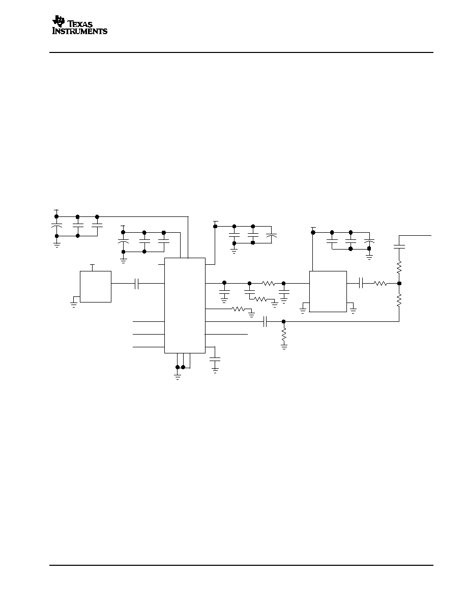
Figure 26. Example Application of the TRF3750 for GSM Wireless Infrastructure Transceivers
Application Example for Direct IQ Upconversion Wireless Infrastructure Transmitter
Much in the same way as described above, the TRF3750 is an ideal synthesizer to use in implementing a
complete direct upconversion transmitter. Using a complete suite of high performance Texas Instruments
components, a state-of-the-art transmitter can be implemented featuring excellent performance. Texas
Instruments offers ideal solutions for the DSP portion of transceivers, for the digital upconverters,
serializers/deserializers, and for the analog, mixed-signal, and RF components needed to complete the
transmitter. The baseband digital data is converted to I and Q signals through the dual DAC5686, which features
offset and gain adjustments in order to optimize the carrier and sideband suppressions of the direct IQ
modulator. If additional gain is desired at the output of the DAC or if the user’s existing solution does not offer
differential signals, the THS4503 differential amplifier can be used between the DAC and the modulator. The
LO input of the IQ modulator is generated by the TRF3750 synthesizer in combination with an external VCO
centered at the frequency of interest. The same considerations as the ones listed in the previous example still
apply. In addition, the CDC7005 clocking solution can be used to clock the DAC and other portions of the
transmitter. A block diagram of the proposed architecture is shown in Figure 27. For more details, contact Texas
Instruments directly.
相关PDF资料 |
PDF描述 |
|---|---|
| MS27473E22F35SB | CONN PLUG 100POS STRAIGHT W/SCKT |
| M83723/78W20287 | CONN PLUG 28POS STRAIGHT W/PINS |
| M83723/78W20286 | CONN PLUG 28POS STRAIGHT W/PINS |
| MS27484E16B6PD | CONN PLUG 6POS STRAIGHT W/PINS |
| X9241AUSIT1 | IC XDCP QUAD 4X50K EE 20-SOIC |
相关代理商/技术参数 |
参数描述 |
|---|---|
| TRF3750IPWRG4 | 功能描述:时钟合成器/抖动清除器 High Perf Integer-N PLL Freq Synth RoHS:否 制造商:Skyworks Solutions, Inc. 输出端数量: 输出电平: 最大输出频率: 输入电平: 最大输入频率:6.1 GHz 电源电压-最大:3.3 V 电源电压-最小:2.7 V 封装 / 箱体:TSSOP-28 封装:Reel |
| TRF3750IRGP | 功能描述:时钟合成器/抖动清除器 Hi Perform Integer-N PLL Freq Synthsizr RoHS:否 制造商:Skyworks Solutions, Inc. 输出端数量: 输出电平: 最大输出频率: 输入电平: 最大输入频率:6.1 GHz 电源电压-最大:3.3 V 电源电压-最小:2.7 V 封装 / 箱体:TSSOP-28 封装:Reel |
| TRF3750IRGPG4 | 功能描述:时钟合成器/抖动清除器 Hi Perform Integer-N PLL Freq Synthsizr RoHS:否 制造商:Skyworks Solutions, Inc. 输出端数量: 输出电平: 最大输出频率: 输入电平: 最大输入频率:6.1 GHz 电源电压-最大:3.3 V 电源电压-最小:2.7 V 封装 / 箱体:TSSOP-28 封装:Reel |
| TRF3750IRGPR | 功能描述:时钟合成器/抖动清除器 High Perf Integer-N PLL Freq Synth RoHS:否 制造商:Skyworks Solutions, Inc. 输出端数量: 输出电平: 最大输出频率: 输入电平: 最大输入频率:6.1 GHz 电源电压-最大:3.3 V 电源电压-最小:2.7 V 封装 / 箱体:TSSOP-28 封装:Reel |
| TRF3750IRGPRG4 | 功能描述:时钟合成器/抖动清除器 High Perf Integer-N PLL Freq Synth RoHS:否 制造商:Skyworks Solutions, Inc. 输出端数量: 输出电平: 最大输出频率: 输入电平: 最大输入频率:6.1 GHz 电源电压-最大:3.3 V 电源电压-最小:2.7 V 封装 / 箱体:TSSOP-28 封装:Reel |
发布紧急采购,3分钟左右您将得到回复。