- 您现在的位置:买卖IC网 > PDF目录1971 > UPD78F0394GC-8EA-A (Renesas Electronics America)MCU 8BIT 48KB FLASH PDF资料下载
参数资料
| 型号: | UPD78F0394GC-8EA-A |
| 厂商: | Renesas Electronics America |
| 文件页数: | 201/682页 |
| 文件大小: | 0K |
| 描述: | MCU 8BIT 48KB FLASH |
| 标准包装: | 400 |
| 系列: | 78K0/Lx2 |
| 核心处理器: | 78K/0 |
| 芯体尺寸: | 8-位 |
| 速度: | 20MHz |
| 连通性: | 3 线 SIO,I²C,LIN,UART/USART |
| 外围设备: | LCD,LVD,POR,PWM,WDT |
| 输入/输出数: | 40 |
| 程序存储器容量: | 48KB(48K x 8) |
| 程序存储器类型: | 闪存 |
| RAM 容量: | 2K x 8 |
| 电压 - 电源 (Vcc/Vdd): | 1.8 V ~ 5.5 V |
| 数据转换器: | A/D 8x10b |
| 振荡器型: | 内部 |
| 工作温度: | -40°C ~ 85°C |
| 封装/外壳: | 100-LQFP |
| 包装: | 托盘 |
第1页第2页第3页第4页第5页第6页第7页第8页第9页第10页第11页第12页第13页第14页第15页第16页第17页第18页第19页第20页第21页第22页第23页第24页第25页第26页第27页第28页第29页第30页第31页第32页第33页第34页第35页第36页第37页第38页第39页第40页第41页第42页第43页第44页第45页第46页第47页第48页第49页第50页第51页第52页第53页第54页第55页第56页第57页第58页第59页第60页第61页第62页第63页第64页第65页第66页第67页第68页第69页第70页第71页第72页第73页第74页第75页第76页第77页第78页第79页第80页第81页第82页第83页第84页第85页第86页第87页第88页第89页第90页第91页第92页第93页第94页第95页第96页第97页第98页第99页第100页第101页第102页第103页第104页第105页第106页第107页第108页第109页第110页第111页第112页第113页第114页第115页第116页第117页第118页第119页第120页第121页第122页第123页第124页第125页第126页第127页第128页第129页第130页第131页第132页第133页第134页第135页第136页第137页第138页第139页第140页第141页第142页第143页第144页第145页第146页第147页第148页第149页第150页第151页第152页第153页第154页第155页第156页第157页第158页第159页第160页第161页第162页第163页第164页第165页第166页第167页第168页第169页第170页第171页第172页第173页第174页第175页第176页第177页第178页第179页第180页第181页第182页第183页第184页第185页第186页第187页第188页第189页第190页第191页第192页第193页第194页第195页第196页第197页第198页第199页第200页当前第201页第202页第203页第204页第205页第206页第207页第208页第209页第210页第211页第212页第213页第214页第215页第216页第217页第218页第219页第220页第221页第222页第223页第224页第225页第226页第227页第228页第229页第230页第231页第232页第233页第234页第235页第236页第237页第238页第239页第240页第241页第242页第243页第244页第245页第246页第247页第248页第249页第250页第251页第252页第253页第254页第255页第256页第257页第258页第259页第260页第261页第262页第263页第264页第265页第266页第267页第268页第269页第270页第271页第272页第273页第274页第275页第276页第277页第278页第279页第280页第281页第282页第283页第284页第285页第286页第287页第288页第289页第290页第291页第292页第293页第294页第295页第296页第297页第298页第299页第300页第301页第302页第303页第304页第305页第306页第307页第308页第309页第310页第311页第312页第313页第314页第315页第316页第317页第318页第319页第320页第321页第322页第323页第324页第325页第326页第327页第328页第329页第330页第331页第332页第333页第334页第335页第336页第337页第338页第339页第340页第341页第342页第343页第344页第345页第346页第347页第348页第349页第350页第351页第352页第353页第354页第355页第356页第357页第358页第359页第360页第361页第362页第363页第364页第365页第366页第367页第368页第369页第370页第371页第372页第373页第374页第375页第376页第377页第378页第379页第380页第381页第382页第383页第384页第385页第386页第387页第388页第389页第390页第391页第392页第393页第394页第395页第396页第397页第398页第399页第400页第401页第402页第403页第404页第405页第406页第407页第408页第409页第410页第411页第412页第413页第414页第415页第416页第417页第418页第419页第420页第421页第422页第423页第424页第425页第426页第427页第428页第429页第430页第431页第432页第433页第434页第435页第436页第437页第438页第439页第440页第441页第442页第443页第444页第445页第446页第447页第448页第449页第450页第451页第452页第453页第454页第455页第456页第457页第458页第459页第460页第461页第462页第463页第464页第465页第466页第467页第468页第469页第470页第471页第472页第473页第474页第475页第476页第477页第478页第479页第480页第481页第482页第483页第484页第485页第486页第487页第488页第489页第490页第491页第492页第493页第494页第495页第496页第497页第498页第499页第500页第501页第502页第503页第504页第505页第506页第507页第508页第509页第510页第511页第512页第513页第514页第515页第516页第517页第518页第519页第520页第521页第522页第523页第524页第525页第526页第527页第528页第529页第530页第531页第532页第533页第534页第535页第536页第537页第538页第539页第540页第541页第542页第543页第544页第545页第546页第547页第548页第549页第550页第551页第552页第553页第554页第555页第556页第557页第558页第559页第560页第561页第562页第563页第564页第565页第566页第567页第568页第569页第570页第571页第572页第573页第574页第575页第576页第577页第578页第579页第580页第581页第582页第583页第584页第585页第586页第587页第588页第589页第590页第591页第592页第593页第594页第595页第596页第597页第598页第599页第600页第601页第602页第603页第604页第605页第606页第607页第608页第609页第610页第611页第612页第613页第614页第615页第616页第617页第618页第619页第620页第621页第622页第623页第624页第625页第626页第627页第628页第629页第630页第631页第632页第633页第634页第635页第636页第637页第638页第639页第640页第641页第642页第643页第644页第645页第646页第647页第648页第649页第650页第651页第652页第653页第654页第655页第656页第657页第658页第659页第660页第661页第662页第663页第664页第665页第666页第667页第668页第669页第670页第671页第672页第673页第674页第675页第676页第677页第678页第679页第680页第681页第682页
CHAPTER 1 OUTLINE
User’s Manual U17473EJ2V0UD
26
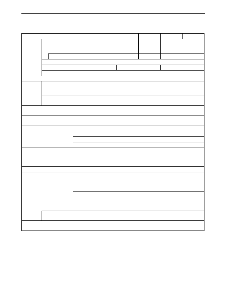
1.8 Outline of Functions
(1/2)
Item
μPD78F0393 μPD78F0394 μPD78F0395 μPD78F0396 μPD78F0397 μPD78F0397D
Flash memory
(self-programming
supported)
Note 1
32 K
48 K
60 K
96 K
128 K
Bank
Note 2
4
6
High-speed RAM
Note 1
1 K
Expansion RAM
Note 1
1 K
2 K
4 K
6 K
Internal
memory
(bytes)
LCD display RAM
40
× 4 bits
Memory space
64 KB
High-speed system
clock
X1 (crystal/ceramic) oscillation, external main system clock input (EXCLK)
1 to 20 MHz: VDD = 4.0 to 5.5 V, 1 to 10 MHz: VDD = 2.7 to 5.5 V,
1 to 5 MHz: VDD = 1.8 to 5.5 V
Main system
clock
(oscillation
frequency)
Internal high-speed
oscillation clock
Internal oscillation
8 MHz (TYP.): VDD = 1.8 to 5.5 V
Subsystem clock
(oscillation frequency)
XT1 (crystal) oscillation, external subsystem clock input (EXCLKS)
32.768 kHz (TYP.): VDD = 1.8 to 5.5 V
Internal low-speed oscillation clock
(for TMH1, WDT)
Internal oscillation
240 kHz (TYP.): VDD = 1.8 to 5.5 V
General-purpose registers
8 bits
× 32 registers (8 bits × 8 registers × 4 banks)
0.1
μs (high-speed system clock: @ fXH = 20 MHz operation)
0.25
μs (internal high-speed oscillation clock: @ fRH = 8 MHz (TYP.) operation)
Minimum instruction execution time
122
μs (subsystem clock: @ fSUB = 32.768 kHz operation)
Instruction set
16-bit operation
Multiply/divide (8 bits
× 8 bits, 16 bits ÷ 8 bits)
Bit manipulate (set, reset, test, and Boolean operation)
BCD adjust, etc.
I/O ports
CMOS I/O: 40
16-bit
timer/event
counter:
1 channel
16-bit timer/event counter: 2 channels
Timers
8-bit timer/event counter: 2 channels
8-bit timer: 2 channels
Watch timer: 1 channel
Watchdog timer: 1 channel
Timer outputs
5 (PWM
output: 4)
6 (PWM output: 4)
Clock output
156.25 kHz, 312.5 kHz (peripheral hardware clock: @ fPRS = 20 MHz operation)
32.768 kHz (subsystem clock: @ fSUB = 32.768 kHz operation)
Notes 1. The internal flash memory capacity, internal high-speed RAM capacity, and internal expansion RAM
capacity can be changed using the internal memory size switching register (IMS) and the internal
expansion RAM size switching register (IXS).
2. Banks to be used can be changed using the bank select register (BANK).
相关PDF资料 |
PDF描述 |
|---|---|
| UPD78F1146AF1-AN1-A | MCU 16BIT 78K0R/KX3 64-FBGA |
| UPD78F1156AGC-GAD-AX | MCU 16BIT 78K0R/KX3 80-LQFP |
| UPD78F1168AGF-GAS-AX | MCU 16BIT 78K0R/KX3 100-LQFP |
| UPD78F1178AGF-GAT-AX | MCU 16BIT 78K0R/KX3 128-LQFP |
| UPD78F1188AGJ-GAE-AX | MCU 16BIT 78K0R/KX3 144-LQFP |
相关代理商/技术参数 |
参数描述 |
|---|---|
| UPD78F0395GC(R)-8EA-A | 制造商:Renesas Electronics Corporation 功能描述: |
| UPD78F0395GC(T)-8EA | 制造商:Renesas Electronics Corporation 功能描述: |
| UPD78F0395GC(T)-8EA-A | 制造商:Renesas Electronics Corporation 功能描述: |
| UPD78F0397DGC(T)-8EA | 制造商:Renesas Electronics Corporation 功能描述: |
| UPD78F0397DGC(T)-8EA-A | 制造商:Renesas Electronics Corporation 功能描述: |
发布紧急采购,3分钟左右您将得到回复。