- 您现在的位置:买卖IC网 > PDF目录202171 > V54C3128164VBI6 (PROMOS TECHNOLOGIES INC) 8M X 16 SYNCHRONOUS DRAM, 5.4 ns, PDSO54 PDF资料下载
参数资料
| 型号: | V54C3128164VBI6 |
| 厂商: | PROMOS TECHNOLOGIES INC |
| 元件分类: | DRAM |
| 英文描述: | 8M X 16 SYNCHRONOUS DRAM, 5.4 ns, PDSO54 |
| 封装: | GREEN, PLASTIC, TSOP2-54 |
| 文件页数: | 8/56页 |
| 文件大小: | 734K |
| 代理商: | V54C3128164VBI6 |
第1页第2页第3页第4页第5页第6页第7页当前第8页第9页第10页第11页第12页第13页第14页第15页第16页第17页第18页第19页第20页第21页第22页第23页第24页第25页第26页第27页第28页第29页第30页第31页第32页第33页第34页第35页第36页第37页第38页第39页第40页第41页第42页第43页第44页第45页第46页第47页第48页第49页第50页第51页第52页第53页第54页第55页第56页
16
V54C3128(16/80/40)4VB Rev.1.5 March 2006
ProMOS TECHNOLOGIES
V54C3128(16/80/40)4VB
Auto Precharge
Two methods are available to precharge SDRAMs. In an automatic precharge mode, the CAS timing ac-
cepts one extra address, CA10, to determine whether the chip restores or not after the operation. If CA10 is
high when a Read Command is issued, the Read with Auto-Precharge function is initiated. The SDRAM
automatically enters the precharge operation one clock before the last data out for CAS latencies 2, two
clocks for CAS latencies 3 and three clocks for CAS latencies 4. If CA10 is high when a Write Command is
issued, the Write with Auto-Precharge function is initiated. The SDRAM automatically enters the precharge
operation a time delay equal to tWR (Write recovery time) after the last data in. Auto-Precharge does not
apply to full-page burst mode.
Precharge Command
There is also a separate precharge command available. When RAS and WE are low and CAS is high at a
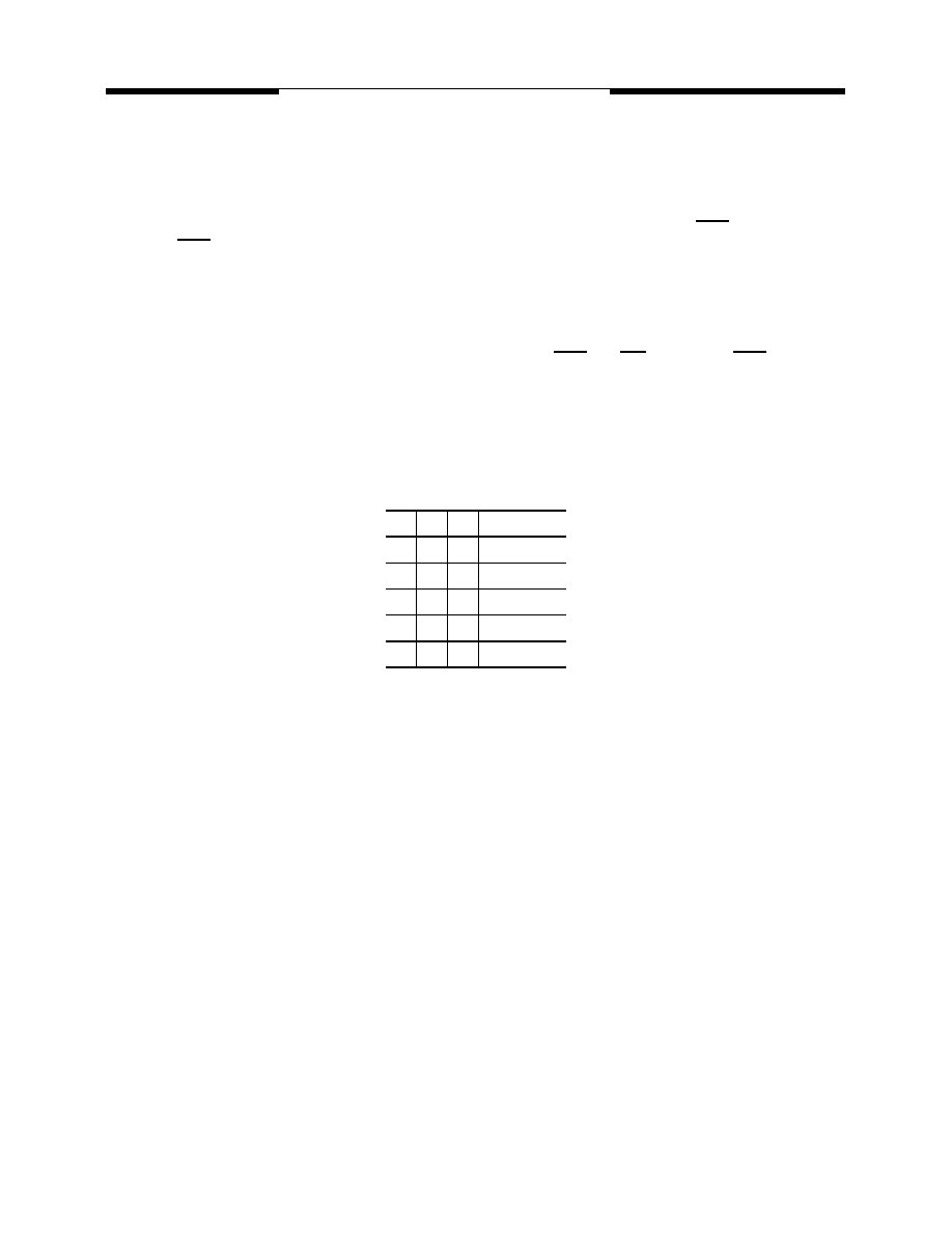
clock timing, it triggers the precharge operation. Three address bits, BA0, BA1 and A10 are used to define
banks as shown in the following list. The precharge command can be imposed one clock before the last data
out for CAS latency = 2, two clocks before the last data out for CAS latency = 3. Writes require a time delay
twr from the last data out to apply the precharge command. A full-page burst may be truncated with a Pre-
charge command to the same bank.
Bank Selection by Address Bits:
Burst Termination
Once a burst read or write operation has been initiated, there are several methods in which to terminate
the burst operation prematurely. These methods include using another Read or Write Command to interrupt
an existing burst operation, use a Precharge Command to interrupt a burst cycle and close the active bank,
or using the Burst Stop Command to terminate the existing burst operation but leave the bank open for future
Read or Write Commands to the same page of the active bank. When interrupting a burst with another Read
or Write Command care must be taken to avoid I/O contention. The Burst Stop Command, however, has the
fewest restrictions making it the easiest method to use when terminating a burst operation before it has been
completed. If a Burst Stop command is issued during a burst write operation, then any residual data from the
burst write cycle will be ignored. Data that is presented on the I/O pins before the Burst Stop Command is
registered will be written to the memory. The full-page burst is used in conjunction with Burst Terminate Com-
mand to generate arbitrary burst lengths.
A10
BA0
BA1
0
Bank 0
0
1
Bank 1
0
1
0
Bank 2
0
1
Bank 3
1
X
all Banks
相关PDF资料 |
PDF描述 |
|---|---|
| V54C3128164VBS8PC | 8M X 16 SYNCHRONOUS DRAM, 6 ns, PBGA60 |
| V54C3128804VAS7PC | 16M X 8 SYNCHRONOUS DRAM, 5.4 ns, PBGA60 |
| V54C3128804VCLC7E | 16M X 8 SYNCHRONOUS DRAM, 7 ns, PBGA54 |
| V54C3128804VCT7PCE | 16M X 8 SYNCHRONOUS DRAM, 7 ns, PDSO54 |
| V54C316162VAT10 | 1M X 16 SYNCHRONOUS DRAM, 8 ns, PDSO50 |
相关代理商/技术参数 |
参数描述 |
|---|---|
| V54C3128164VBI7 | 制造商:PROMOS 功能描述: 制造商:ProMOS Technologies Inc 功能描述:8M X 16 SYNCHRONOUS DRAM, 5.4 ns, PDSO54 |
| V54C3128164VS | 制造商:MOSEL 制造商全称:MOSEL 功能描述:128Mbit SDRAM 3.3 VOLT, TSOP II / SOC PACKAGE 8M X 16, 16M X 8, 32M X 4 |
| V54C3128164VT | 制造商:MOSEL 制造商全称:MOSEL 功能描述:128Mbit SDRAM 3.3 VOLT, TSOP II / SOC PACKAGE 8M X 16, 16M X 8, 32M X 4 |
| V54C3128404VBGA | 制造商:MOSEL 制造商全称:MOSEL 功能描述:128Mbit SDRAM 3.3 VOLT, BGA PACKAGE |
| V54C3128404VS | 制造商:MOSEL 制造商全称:MOSEL 功能描述:128Mbit SDRAM 3.3 VOLT, TSOP II / SOC PACKAGE 8M X 16, 16M X 8, 32M X 4 |
发布紧急采购,3分钟左右您将得到回复。