- 您现在的位置:买卖IC网 > PDF目录297710 > V826632K24S (Mosel Vitelic, Corp.) 2.5 VOLT 32M x 64 HIGH PERFORMANCE UNBUFFERED DDR SDRAM MODULE PDF资料下载
参数资料
| 型号: | V826632K24S |
| 厂商: | Mosel Vitelic, Corp. |
| 英文描述: | 2.5 VOLT 32M x 64 HIGH PERFORMANCE UNBUFFERED DDR SDRAM MODULE |
| 中文描述: | 2.5伏32M的高性能× 64 DDR SDRAM内存模块缓冲 |
| 文件页数: | 2/14页 |
| 文件大小: | 126K |
| 代理商: | V826632K24S |
10
V826632K24S Rev. 1.0 April 2002
MOSEL VITELIC
V826632K24S
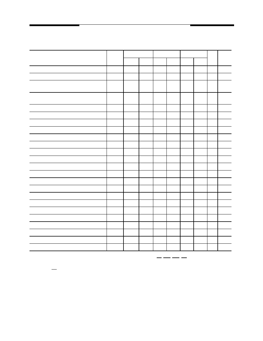
AC Characteristics (cont.)
Notes: 1. This calculation accounts for tDQSQ(max), the pulse width distortion of on-chip circuit and jitter.
2. Data sampled at the rising edges of the clock : A0~A11, BA0~BA1, CKE, CS, RAS, CAS, WE.
3. For command/address input slew rate >=1.0V/ns
4. For command/address input slew rate >=0.5V/ns and <1.0V/ns
5. CK, CK slew rates are >=1.0V/ns
6. These parameters guarantee device timing, but they are not necessarily tested on each device, and they may be guaranteed
by design or tester correlation.
7. Data latched at both rising and falling edges of Data Strobes(DQS) : DQ, DM
8. Minimum of 200 cycles of stable input clocks after Self Refresh Exit command, where CKE is held high, is required to complete
Self Refresh Exit and lock the internal DLL circuit of DDR SDRAM.
DQS-Out edge to Clock edge Skew
tDQSCK
-0.75
0.75
-0.75
0.75
-0.8
0.8
ns
DQS-Out edge to Data-Out edge Skew
tDQSQ
-
0.5
-
0.5
-
0.6
ns
Data-Out hold time from DQS
tQH
tHPmin
-0.75ns
-
tHPmin
-0.75ns
-
tHPmin
-0.75ns
-
ns
1
Clock Half Period
tHP
tCH/L
min
-
tCH/L
min
-
tCH/L
min
-
ns
1
Input Setup Time (fast slew rate)
tIS
0.9
-
0.9
-
1.1
-
ns
2,3,5,6
Input Hold Time (fast slew rate)
tIH
0.9
-
0.9
-
1.1
-
ns
2,3,5,6
Input Setup Time (slow slew rate)
tIS
1.0
-
1.0
-
1.1
-
ns
2,4,5,6
Input Hold Time (slow slew rate)
tIH
1.0
-
1.0
-
1.1
-
ns
2,4,5,6
Write DQS High Level Width
tDQSH
0.4
0.6
0.4
0.6
0.4
0.6
CLK
Write DQS Low Level Width
tDQSL
0.4
0.6
0.4
0.6
0.4
0.6
CLK
CLK to First Rising edge of DQS-In
tDQSS
0.75
1.25
0.75
1.25
0.75
1.25
CLK
Data-In Setup Time to DQS-In (DQ & DM)
tDS
0.5
-
0.5
-
0.6
-
ns
7
Data-in Hold Time to DQS-In (DQ & DM)
tDH
0.5
-
0.5
-
0.6
-
ns
7
DQ & DM Input Pulse Width
tDIPW
1.75
-
1.75
-
2
-
ns
Read DQS Preamble Time
tRPRE
0.9
1.1
0.9
1.1
0.9
1.1
CLK
Read DQS Postamble Time
tRPST
0.4
0.6
0.4
0.6
0.4
0.6
CLK
Write DQS Preamble Setup Time
tWPRES
0
-
0
-
0
-
CLK
Write DQS Preamble Hold Time
tWPREH
0.25
-
0.25
-
0.25
-
CLK
Write DQS Postamble Time
tWPST
0.4
0.6
0.4
0.6
0.4
0.6
CLK
Mode Register Set Delay
tMRD
2
-
2
-
2
-
CLK
Power Down Exit Time
tPDEX
10
-
10
-
10
-
ns
Exit Self Refresh to Non-Read Command
tXSNR
75
-
75
-
80
-
ns
Exit Self Refresh to Read Command
tXSRD
200
-
200
-
200
-
CLK
8
Average Periodic Refresh Interval
tREFI
-
7.8
-
7.8
-
7.8
us
Parameter
Symbol
(PC266A)
(PC266B)
(PC200)
Unit
Note
Min
Max
Min
Max
Min
Max
相关PDF资料 |
PDF描述 |
|---|---|
| V827332U04S | 2.5 VOLT 32M x 72 HIGH PERFORMANCE REGISTERED ECC DDR SDRAM MODULE |
| V827432K24SAEX-B1 | 32M X 72 DDR DRAM MODULE, 0.75 ns, DMA184 |
| V827432K24S | 2.5 VOLT 32M x 72 HIGH PERFORMANCE UNBUFFERED ECC DDR SDRAM MODULE |
| V85ECADBFREQ | VCXO, CLOCK, 1.5 MHz - 200 MHz, HCMOS OUTPUT |
| V85ECBDAFREQ | VCXO, CLOCK, 1.5 MHz - 200 MHz, HCMOS OUTPUT |
相关代理商/技术参数 |
参数描述 |
|---|---|
| V826664G24S | 制造商:MOSEL 制造商全称:MOSEL 功能描述:512 MB 200-PIN DDR UNBUFFERED SODIMM 2.5 VOLT 64M x 64 |
| V826664K24S | 制造商:MOSEL 制造商全称:MOSEL 功能描述:2.5 VOLT 64M x 64 HIGH PERFORMANCE UNBUFFERED DDR SDRAM MODULE |
| V827316K04S | 制造商:MOSEL 制造商全称:MOSEL 功能描述:2.5 VOLT 16M x 72 HIGH PERFORMANCE UNBUFFERED ECC DDR SDRAM MODULE |
| V827332K04S | 制造商:MOSEL 制造商全称:MOSEL 功能描述:2.5 VOLT 32M x 72 HIGH PERFORMANCE UNBUFFERED ECC DDR SDRAM MODULE |
| V827332N04S | 制造商:MOSEL 制造商全称:MOSEL 功能描述:2.5 VOLT 32M x 72 HIGH PERFORMANCE REGISTERED ECC DDR SDRAM MODULE |
发布紧急采购,3分钟左右您将得到回复。