- 您现在的位置:买卖IC网 > PDF目录300087 > VCA2615RGZR (TEXAS INSTRUMENTS INC) SPECIALTY ANALOG CIRCUIT, PQCC48 PDF资料下载
参数资料
| 型号: | VCA2615RGZR |
| 厂商: | TEXAS INSTRUMENTS INC |
| 元件分类: | 模拟信号调理 |
| 英文描述: | SPECIALTY ANALOG CIRCUIT, PQCC48 |
| 封装: | 7 X 7 MM, GREEN, PLASTIC, QFN-48 |
| 文件页数: | 7/33页 |
| 文件大小: | 1122K |
| 代理商: | VCA2615RGZR |
第1页第2页第3页第4页第5页第6页当前第7页第8页第9页第10页第11页第12页第13页第14页第15页第16页第17页第18页第19页第20页第21页第22页第23页第24页第25页第26页第27页第28页第29页第30页第31页第32页第33页
VCA2615
SBOS316D JULY 2005 REVISED OCTOBER 2008
www.ti.com
15
THEORY OF OPERATION
The VCA2615 is a dual-channel system consisting of two
primary blocks: a low noise preamplifier (LNP) and a
variable gain amplifier (VGA), which is driven from the
LNP. The LNP is very flexible; both the gain and input
impedance can be programmed digitally without using
external components. The LNP is coupled to the VGA
through a multiplexer to facilitate interfacing with an
external signal processor. The VGA is a true variable-gain
amplifier, achieving lower noise output at lower gains. The
output amplifier has two gains, allowing for further
optimization with different analog-to-digital converters.
Figure 53 shows a simplified block diagram of a single
channel of the dual-channel system. Both the LNP and the
VGA can be powered down together or separately in order
to conserve system power when necessary.
LNP
VGA
Figure 53. Simplified Block Diagram of VCA2615
LNP—OVERVIEW
The LNP has differential input and output capability. It also
has exceptionally low noise voltage and input current
noise. At the highest gain setting (of 22dB), the LNP
achieves 0.7nV/
√Hz voltage noise and typically 1pA/√Hz
current noise. The LNP can process fully differential or
single-ended signals in each channel. Differential signal
processing reduces second harmonic distortion and offers
improved rejection of common-mode and power-supply
noise. The LNP gain can be electronically programmed to
have one of four values that can be selected by a two-bit
word (see Table 2). The gain of the LNP when driving the
VGA is approximately 1dB higher because of the loss in
the buffer.
The LNP also has four programmable feedback resistors
that can be selected by a four-bit word to create 16 different
values in order to facilitate the easy use of active feedback.
With this combination of both programmable gain and
feedback resistors, as many as 61 different values of input
impedance can be created to provide a wide variety of
input-matching resistors (see Table 5). By using active
feedback with this wide selection of feedback resistors, the
user is able to provide a low-noise means of terminating
input
signal
while
incurring
only
a
3dB
loss
in
signal-to-noise ratio (SNR), instead of a 6dB loss in SNR
which is usually associated with the conventional type of
signal termination. More information is given in the section
of this document that provides a detailed description of the
LNP.
The LNP output drives a buffer that in turn drives the
feedback network and supplies the LNP to a multiplexer.
The multiplexer can be configured to supply the signal
off-chip for further processing, or can be set to drive the
internal VGA directly from the LNP. An external coupling
capacitor is not required to couple the LNP to the VGA.
VGA—OVERVIEW
The VGA that is used with the VCA2615 is a true
variable-gain amplifier; as the gain is reduced, the noise
contribution from the VGA itself is also reduced. A block
diagram of the VGA is shown in Figure 53. This design is
in contrast with another popular device architecture (used
by the VCA2616), where an effective VCA characteristic
is obtained by a voltage variable-attenuator succeeded by
a fixed-gain amplifier. At the highest gain, systems with
either architecture are dominated by the noise produced
by the LNP. At low gains, however, the noise output is
dominated by the contribution from the VGA. Therefore,
the overall system with lower VGA gain will produce less
noise.
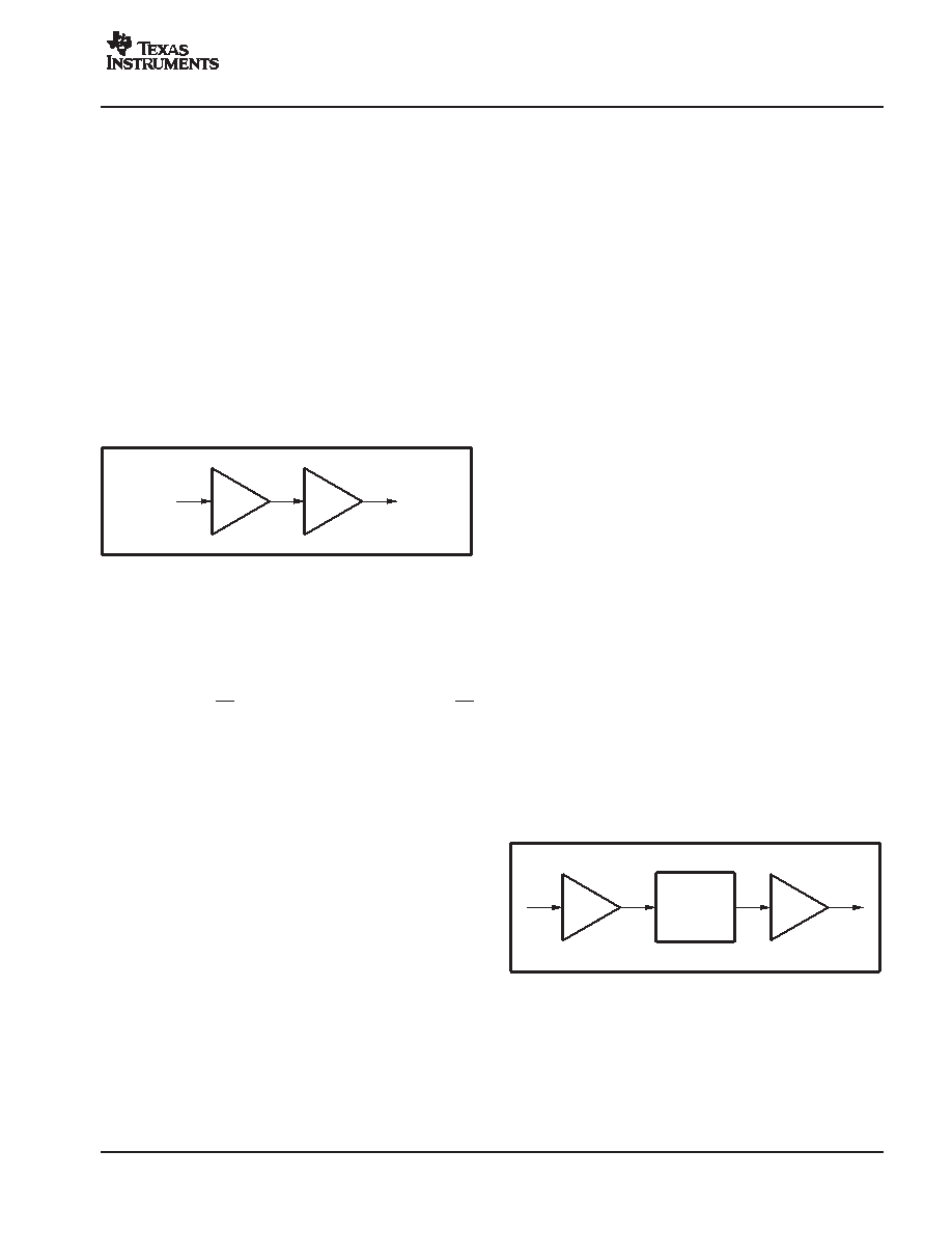
The following example will illustrate this point. Figure 53
shows a block diagram of an LNP driving a variable-gain
amplifier; Figure 54 shows a block diagram of an LNP
driving a variable attenuation attenuator followed by a
fixed gain amplifier. For purposes of this example, let us
assume the performance characteristics shown in Table 1;
these values are the typical performance data of the
VCA2615 and the VCA2616.
LNP
Amplifier
ATTENUATOR
Figure 54. Block Diagram of Older VCA Models
相关PDF资料 |
PDF描述 |
|---|---|
| VCA3-103-60M00 | CRYSTAL OSCILLATOR, CLOCK, 60 MHz, HCMOS/TTL OUTPUT |
| VCA3-A3F-FREQ | CRYSTAL OSCILLATOR, CLOCK, 0.32768 MHz - 160 MHz, CMOS OUTPUT |
| VCA3-A5D-FREQ | CRYSTAL OSCILLATOR, CLOCK, 0.32768 MHz - 160 MHz, CMOS OUTPUT |
| VCA3-C3H-FREQ | CRYSTAL OSCILLATOR, CLOCK, 0.32768 MHz - 160 MHz, CMOS OUTPUT |
| VCA3-F3G-FREQ | CRYSTAL OSCILLATOR, CLOCK, 0.32768 MHz - 160 MHz, CMOS OUTPUT |
相关代理商/技术参数 |
参数描述 |
|---|---|
| VCA2615RGZRG4 | 功能描述:特殊用途放大器 2-Channel Variable Gain Amplifier RoHS:否 制造商:Texas Instruments 通道数量:Single 共模抑制比(最小值): 输入补偿电压: 工作电源电压:3 V to 5.5 V 电源电流:5 mA 最大功率耗散: 最大工作温度:+ 70 C 最小工作温度:- 40 C 安装风格:SMD/SMT 封装 / 箱体:QFN-20 封装:Reel |
| VCA2615RGZT | 功能描述:特殊用途放大器 2-Channel Variable Gain Amplifier RoHS:否 制造商:Texas Instruments 通道数量:Single 共模抑制比(最小值): 输入补偿电压: 工作电源电压:3 V to 5.5 V 电源电流:5 mA 最大功率耗散: 最大工作温度:+ 70 C 最小工作温度:- 40 C 安装风格:SMD/SMT 封装 / 箱体:QFN-20 封装:Reel |
| VCA2615RGZTG4 | 功能描述:特殊用途放大器 2-Channel Variable Gain Amplifier RoHS:否 制造商:Texas Instruments 通道数量:Single 共模抑制比(最小值): 输入补偿电压: 工作电源电压:3 V to 5.5 V 电源电流:5 mA 最大功率耗散: 最大工作温度:+ 70 C 最小工作温度:- 40 C 安装风格:SMD/SMT 封装 / 箱体:QFN-20 封装:Reel |
| VCA2616 | 制造商:BB 制造商全称:BB 功能描述:Dual, Variable-Gain Amplifier with Low-Noise Preamp |
| VCA2616EVM | 功能描述:放大器 IC 开发工具 VCA2616 Eval Mod RoHS:否 制造商:International Rectifier 产品:Demonstration Boards 类型:Power Amplifiers 工具用于评估:IR4302 工作电源电压:13 V to 23 V |
发布紧急采购,3分钟左右您将得到回复。