- 您现在的位置:买卖IC网 > PDF目录300087 > VCA2615RGZR (TEXAS INSTRUMENTS INC) SPECIALTY ANALOG CIRCUIT, PQCC48 PDF资料下载
参数资料
| 型号: | VCA2615RGZR |
| 厂商: | TEXAS INSTRUMENTS INC |
| 元件分类: | 模拟信号调理 |
| 英文描述: | SPECIALTY ANALOG CIRCUIT, PQCC48 |
| 封装: | 7 X 7 MM, GREEN, PLASTIC, QFN-48 |
| 文件页数: | 8/33页 |
| 文件大小: | 1122K |
| 代理商: | VCA2615RGZR |
第1页第2页第3页第4页第5页第6页第7页当前第8页第9页第10页第11页第12页第13页第14页第15页第16页第17页第18页第19页第20页第21页第22页第23页第24页第25页第26页第27页第28页第29页第30页第31页第32页第33页
VCA2615
SBOS316D JULY 2005 REVISED OCTOBER 2008
www.ti.com
16
Table 1. Gain and Noise Performance of Various
VCA Blocks
BLOCK
GAIN (Loss) dB
NOISE nV/
√Hz
LNP1 (VCA2615)
20
0.82
LNP2 (VCA2616)
20
1.1
Attenuator (VCA2616)
0
1.8
Attenuator (VCA2616)
40
1.8
VCA1 (VCA2615)
40
3.8
VCA1 (VCA2615)
0
90
VCA2 (VCA2616)
40
2.0
When the block diagram shown in Figure 53 has a
combined gain of 60dB, the noise referred to the input
(RTI) is given by the expression:
Total Noise (RTI)
+ (LNP Noise)2 ) (VCA Noise LNP Gain)2
+ (0.82)2 ) (3.8 10)2 + 0.90nV Hz
When the block diagram shown in Figure 54 has the
combined gain of 60dB, the noise referred to the input
(RTI) is given by the expression:
Total Noise (RTI)
+
(LNP Noise)2
) (ATTEN Noise LNP Gain)2 ) (VCA Noise LNP Gain)2
+ (1.1)2 ) (1.8 10)2 ) (2.0 10)2 + 1.13nV
Hz
Repeating the above measurements for both VCA
configurations when the overall gain is 20dB yields the
following results:
For the VCA with a variable gain amplifier (Figure 53):
Total Noise (RTI)
+ (0.82)2 ) (90 10)2 + 9.03nV Hz
For the VCA with a variable attenuation attenuator
(Figure 54):
Total Noise
+ (1.1)2 ) (1.8 10)2 ) (2.0 0.10)2
+ 14nV Hz
The VGA has a continuously-variable gain range of 52dB
with the ability to select either of two options. The gain of
the VGA can either be varied from 12dB to 40dB, or from
18dB to 34dB. The VGA output can be programmed to
clip precisely at a predetermined voltage that is selected
by the user. When the user applies a voltage to pin 18
(VCLMP), the output will have a peak-to-peak voltage that is
given by the graph shown in Figure 48.
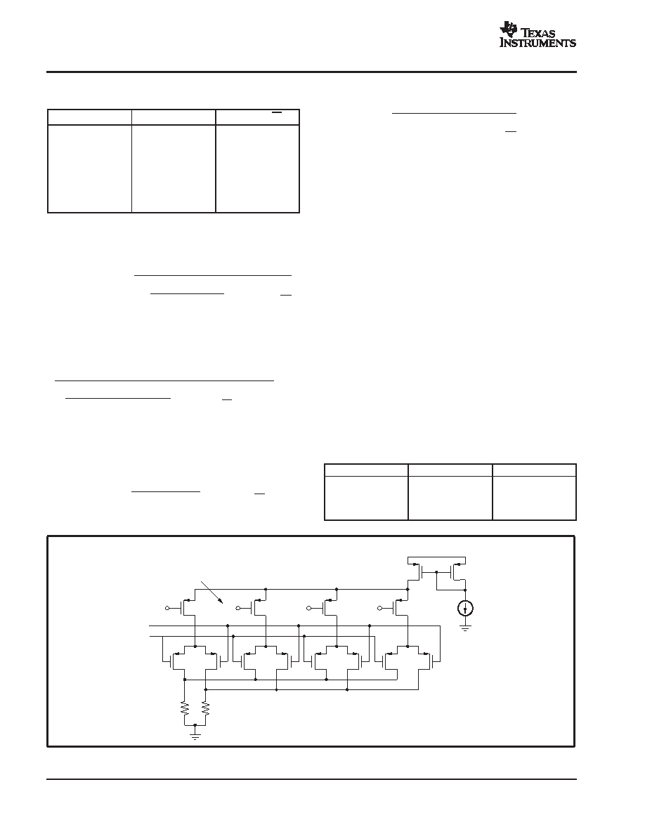
LOW NOISE PREAMPLIFIER (LNP)—DETAIL
The LNP is designed to achieve exceptionally low noise
performance when employed with or without active
feedback. The proprietary LNP architecture can be
electronically programmed, eliminating the need for
off-board components to alter the gain. A simplified
schematic of this amplifier is shown in Figure 55. FET pairs
Q1Q2, Q3Q4, Q5Q6 and Q7Q8 each represent a
different LNP gain. The four switches are 22dB, 18dB,
12dB and 3dB. One of the unique gain settings is selected
when one of the four switches Q9 through Q12 are
selected. Table 2 shows the relationship between the gain
selection bits, G1 and G2, and the corresponding gain.
Table 2. Gain Selection of LNP
G1
G2
LNP GAIN (dB)
0
3
0
1
12
1
0
18
1
22
Q9
Digital Gain Select
IN
+IN
OUT
+OUT
Q1
Q2
Q10
Q3
Q4
Q11
Q5
Q6
Q12
VDD
Q7
Q13
Q14
Q8
Figure 55. Programmable LNP
(1)
(2)
(3)
(4)
相关PDF资料 |
PDF描述 |
|---|---|
| VCA3-103-60M00 | CRYSTAL OSCILLATOR, CLOCK, 60 MHz, HCMOS/TTL OUTPUT |
| VCA3-A3F-FREQ | CRYSTAL OSCILLATOR, CLOCK, 0.32768 MHz - 160 MHz, CMOS OUTPUT |
| VCA3-A5D-FREQ | CRYSTAL OSCILLATOR, CLOCK, 0.32768 MHz - 160 MHz, CMOS OUTPUT |
| VCA3-C3H-FREQ | CRYSTAL OSCILLATOR, CLOCK, 0.32768 MHz - 160 MHz, CMOS OUTPUT |
| VCA3-F3G-FREQ | CRYSTAL OSCILLATOR, CLOCK, 0.32768 MHz - 160 MHz, CMOS OUTPUT |
相关代理商/技术参数 |
参数描述 |
|---|---|
| VCA2615RGZRG4 | 功能描述:特殊用途放大器 2-Channel Variable Gain Amplifier RoHS:否 制造商:Texas Instruments 通道数量:Single 共模抑制比(最小值): 输入补偿电压: 工作电源电压:3 V to 5.5 V 电源电流:5 mA 最大功率耗散: 最大工作温度:+ 70 C 最小工作温度:- 40 C 安装风格:SMD/SMT 封装 / 箱体:QFN-20 封装:Reel |
| VCA2615RGZT | 功能描述:特殊用途放大器 2-Channel Variable Gain Amplifier RoHS:否 制造商:Texas Instruments 通道数量:Single 共模抑制比(最小值): 输入补偿电压: 工作电源电压:3 V to 5.5 V 电源电流:5 mA 最大功率耗散: 最大工作温度:+ 70 C 最小工作温度:- 40 C 安装风格:SMD/SMT 封装 / 箱体:QFN-20 封装:Reel |
| VCA2615RGZTG4 | 功能描述:特殊用途放大器 2-Channel Variable Gain Amplifier RoHS:否 制造商:Texas Instruments 通道数量:Single 共模抑制比(最小值): 输入补偿电压: 工作电源电压:3 V to 5.5 V 电源电流:5 mA 最大功率耗散: 最大工作温度:+ 70 C 最小工作温度:- 40 C 安装风格:SMD/SMT 封装 / 箱体:QFN-20 封装:Reel |
| VCA2616 | 制造商:BB 制造商全称:BB 功能描述:Dual, Variable-Gain Amplifier with Low-Noise Preamp |
| VCA2616EVM | 功能描述:放大器 IC 开发工具 VCA2616 Eval Mod RoHS:否 制造商:International Rectifier 产品:Demonstration Boards 类型:Power Amplifiers 工具用于评估:IR4302 工作电源电压:13 V to 23 V |
发布紧急采购,3分钟左右您将得到回复。