- 您现在的位置:买卖IC网 > PDF目录300087 > VCA2615RGZR (TEXAS INSTRUMENTS INC) SPECIALTY ANALOG CIRCUIT, PQCC48 PDF资料下载
参数资料
| 型号: | VCA2615RGZR |
| 厂商: | TEXAS INSTRUMENTS INC |
| 元件分类: | 模拟信号调理 |
| 英文描述: | SPECIALTY ANALOG CIRCUIT, PQCC48 |
| 封装: | 7 X 7 MM, GREEN, PLASTIC, QFN-48 |
| 文件页数: | 9/33页 |
| 文件大小: | 1122K |
| 代理商: | VCA2615RGZR |
第1页第2页第3页第4页第5页第6页第7页第8页当前第9页第10页第11页第12页第13页第14页第15页第16页第17页第18页第19页第20页第21页第22页第23页第24页第25页第26页第27页第28页第29页第30页第31页第32页第33页
VCA2615
SBOS316D JULY 2005 REVISED OCTOBER 2008
www.ti.com
17
The ability to change the gain electronically offers
additional flexibility for optimizing the gain in order to
achieve either maximum signal-handling capability or
maximum sensitivity. Table 3 lists the input and output
signal-handling capability of the LNP.
Table 4 shows the voltage noise of the LNP for different
gain settings.
Table 3. Signal Handling Capability of LNP
GAIN
(dB)
G1, G2
MAX INPUT
(VPP Single-Ended)
MAX OUTPUT
(VPP Differential)
22
11
0.23
3.5
18
10
0.39
3.5
12
01
0.78
3.5
3
00
2.3
3.0
Table 4. LNP Gain vs Voltage Noise
LNP GAIN (dB)
VOLTAGE NOISE
(nV/
√Hz) at 5MHz
22
0.8
18
1.1
12
1.9
3
4.9
The current noise for the LNP is 1pA/
√Hz for all gain
settings. The input capacitance of the LNP is 45pF.
The LNP output drives a buffer and a multiplexer (MUX)
along with a feedback network that can be used to program
the input impedance. Figure 56 shows a block diagram of
how these circuits are connected together. The output of
the LNP feeds a buffer to avoid the loading effect of the
feedback resistors and to achieve a more robust capability
for driving external circuits.
Buffer
LNP
VGA
OUT
LNP OUT
VGA IN
MUX
IN
Feedback
Resistors
Figure 56. Block Diagram of LNP/VGA Interface
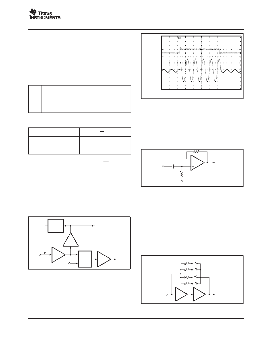
See Figure 57, which shows the response time of the LNP
gain changing from minimum to maximum.
Time (200ns/div)
LNP Gain
11
00
(10V/div)
LNP
Output
(500mV/div)
Figure 57. LNP Gain Change Response
The LNP also feeds a MUX, which accepts the LNP signal
or can receive an external signal. When applying an
external signal to the MUX (VCAIN), the signal should be
biased to a common-mode voltage in the range of 1.85V
to 3.15V. This biasing could be accomplished by using the
2.5V level of the VCM pin (19) of the VCA2615.
To MUX
(VGA
IN)
V
CM
IN
Figure 58. Recommended Circuit for Coupling an
External Signal into the MUX
INPUT IMPEDANCE
Figure 59 shows a simplified schematic of the resistor
feedback network along with Table 5 that relates the FB1,
FB2, FB3 and FB4 code to the selected value. When the
selection bits leave the feedback network in the open
position, the input resistance of the LNP will become
100k
.
LNP
IN
OUT
1500
(FB1)
(FB2)
(FB3)
(FB4)
1000
500
250
Buffer
Figure 59. Feedback Resistor Network
相关PDF资料 |
PDF描述 |
|---|---|
| VCA3-103-60M00 | CRYSTAL OSCILLATOR, CLOCK, 60 MHz, HCMOS/TTL OUTPUT |
| VCA3-A3F-FREQ | CRYSTAL OSCILLATOR, CLOCK, 0.32768 MHz - 160 MHz, CMOS OUTPUT |
| VCA3-A5D-FREQ | CRYSTAL OSCILLATOR, CLOCK, 0.32768 MHz - 160 MHz, CMOS OUTPUT |
| VCA3-C3H-FREQ | CRYSTAL OSCILLATOR, CLOCK, 0.32768 MHz - 160 MHz, CMOS OUTPUT |
| VCA3-F3G-FREQ | CRYSTAL OSCILLATOR, CLOCK, 0.32768 MHz - 160 MHz, CMOS OUTPUT |
相关代理商/技术参数 |
参数描述 |
|---|---|
| VCA2615RGZRG4 | 功能描述:特殊用途放大器 2-Channel Variable Gain Amplifier RoHS:否 制造商:Texas Instruments 通道数量:Single 共模抑制比(最小值): 输入补偿电压: 工作电源电压:3 V to 5.5 V 电源电流:5 mA 最大功率耗散: 最大工作温度:+ 70 C 最小工作温度:- 40 C 安装风格:SMD/SMT 封装 / 箱体:QFN-20 封装:Reel |
| VCA2615RGZT | 功能描述:特殊用途放大器 2-Channel Variable Gain Amplifier RoHS:否 制造商:Texas Instruments 通道数量:Single 共模抑制比(最小值): 输入补偿电压: 工作电源电压:3 V to 5.5 V 电源电流:5 mA 最大功率耗散: 最大工作温度:+ 70 C 最小工作温度:- 40 C 安装风格:SMD/SMT 封装 / 箱体:QFN-20 封装:Reel |
| VCA2615RGZTG4 | 功能描述:特殊用途放大器 2-Channel Variable Gain Amplifier RoHS:否 制造商:Texas Instruments 通道数量:Single 共模抑制比(最小值): 输入补偿电压: 工作电源电压:3 V to 5.5 V 电源电流:5 mA 最大功率耗散: 最大工作温度:+ 70 C 最小工作温度:- 40 C 安装风格:SMD/SMT 封装 / 箱体:QFN-20 封装:Reel |
| VCA2616 | 制造商:BB 制造商全称:BB 功能描述:Dual, Variable-Gain Amplifier with Low-Noise Preamp |
| VCA2616EVM | 功能描述:放大器 IC 开发工具 VCA2616 Eval Mod RoHS:否 制造商:International Rectifier 产品:Demonstration Boards 类型:Power Amplifiers 工具用于评估:IR4302 工作电源电压:13 V to 23 V |
发布紧急采购,3分钟左右您将得到回复。