- 您现在的位置:买卖IC网 > PDF目录11591 > VNC2-64Q1B-REEL (FTDI, Future Technology Devices International Ltd)IC USB HOST/DEVICE CTRL 64-QFN PDF资料下载
参数资料
| 型号: | VNC2-64Q1B-REEL |
| 厂商: | FTDI, Future Technology Devices International Ltd |
| 文件页数: | 47/88页 |
| 文件大小: | 0K |
| 描述: | IC USB HOST/DEVICE CTRL 64-QFN |
| 应用说明: | Vinculum-II IO Cell Description AppNote Vinculum-II Debug Interface Description AppNote Vinculum-II IO Mux Explained AppNote Vinculum-II PWM Example AppNote Migrating Vinculum Designs AppNote |
| 特色产品: | Vinculum VNC2 |
| 标准包装: | 1 |
| 系列: | Vinculum-II |
| 控制器类型: | USB 2.0 控制器 |
| 接口: | USB,主机/设备配置,UART,SPI,PWM,闪存 256K,DMA 4CH |
| 电源电压: | 1.62 V ~ 1.98 V |
| 电流 - 电源: | 25mA |
| 工作温度: | -40°C ~ 85°C |
| 安装类型: | 表面贴装 |
| 封装/外壳: | 64-VFQFN 裸露焊盘 |
| 供应商设备封装: | 64-QFN(8x8) |
| 包装: | 标准包装 |
| 产品目录页面: | 634 (CN2011-ZH PDF) |
| 其它名称: | 768-1046-6 |
第1页第2页第3页第4页第5页第6页第7页第8页第9页第10页第11页第12页第13页第14页第15页第16页第17页第18页第19页第20页第21页第22页第23页第24页第25页第26页第27页第28页第29页第30页第31页第32页第33页第34页第35页第36页第37页第38页第39页第40页第41页第42页第43页第44页第45页第46页当前第47页第48页第49页第50页第51页第52页第53页第54页第55页第56页第57页第58页第59页第60页第61页第62页第63页第64页第65页第66页第67页第68页第69页第70页第71页第72页第73页第74页第75页第76页第77页第78页第79页第80页第81页第82页第83页第84页第85页第86页第87页第88页
51
Copyright 2009-2011 Future Technology Devices International Limited
Datasheet
Vinculum-II Embedded Dual USB Host Controller IC
Version 1.5
Document No.: FT_000138 Clearance No.: FTDI# 143
Status Bit
Meaning
0
New Data
Data in current transaction is valid data.
Byte removed from Transmit Buffer.
1
Old Data
This same data has been read in a previous read cycle.
Repeat the read cycle until New Data is received.
Table 6.10 SPI Master Data Read Status Bit
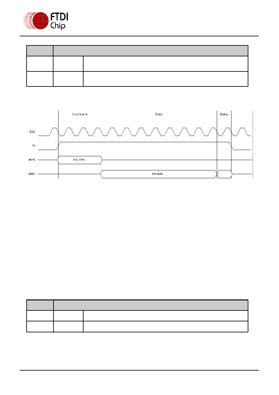
Figure 6.17 SPI Master Data Read (VNC2 Slave Mode)
The status bit is only valid until the next rising edge of SCLK after the last data bit.
During the Data Read operation the SS signal must not be de-asserted.
The transfer completes after 12 clock cycles and the next transfer can begin when MOSI and SS are high
during the rising edge of SCLK.
6.3.6.3 SPI Master Data Write Transaction in VNC1L legacy mode
During an SPI master Data Write operation the Start and Setup sequence is sent by the SPI master to
VNC2, see Figure 6.18. This is followed by the SPI master transmitting each bit of the data to be written
to VNC2. The VNC2 then responds with a status bit on MISO on the rising edge of the next clock cycle.
The SPI master must read the status bit at the end of each write transaction to determine if the data was
written successfully to VNC2 Receive Buffer. The Data Write status bit is defined in Table 6.11.The
status bit is only valid until the next rising edge of SCLK after the last data bit.
If the status bit indicates Accept then the byte transmitted has been added to VNC2 Receive Buffer. If it
shows Reject then the Receive Buffer is full and the byte of data transmitted in the current transaction
should be re-transmitted by the SPI master to VNC2.
Any application should poll VNC2 Receive Buffer by retrying the Data Write operation until the data is
accepted.
Status Bit
Meaning
0
Accept
Data from the current transaction was accepted and added to the Receive Buffer
1
Reject
Write data was not accepted. Retry the same write cycle.
Table 6.11 SPI Master Data Write Status Bit
相关PDF资料 |
PDF描述 |
|---|---|
| V72A48C400BF2 | CONVERTER MOD DC/DC 48V 400W |
| PIC16F1827-E/SO | MCU PIC 8BIT 4K FLASH 18-SOIC |
| PIC16F1826T-I/MV | MCU PIC 8BIT 2K FLASH 28-UQFN |
| PIC16F1826T-I/ML | MCU PIC 8BIT 2K FLASH 28-QFN |
| PIC24F04KA201T-I/MQ | IC PIC MCU FLASH 512KX4 20-QFN |
相关代理商/技术参数 |
参数描述 |
|---|---|
| VNC2-64Q1B-TRAY | 功能描述:USB 接口集成电路 Vinculum-II Dual Host/Dev IC QFN-64 RoHS:否 制造商:Cypress Semiconductor 产品:USB 2.0 数据速率: 接口类型:SPI 工作电源电压:3.15 V to 3.45 V 工作电源电流: 最大工作温度:+ 85 C 安装风格:SMD/SMT 封装 / 箱体:WLCSP-20 |
| VNC2DEBUGMODULE | 制造商:Future Technology Devices International (FTDI Chip) 功能描述:VNC2 Vinculum Debug Module |
| VNC712B-N50A-5TZ | 制造商:SMC Corporation of America 功能描述:Valve, media, coolant, 2 way |
| VNC-DK4-C1404CM | 制造商:L-com Inc 功能描述:4CH DVR w/4 CMOS CAMERAS no HD |
| VNC-DK4-C1404CM-HD | 制造商:L-com Inc 功能描述:4CH DVR w/4 CMOS CAMS 500GB HD |
发布紧急采购,3分钟左右您将得到回复。