- 您现在的位置:买卖IC网 > PDF目录361765 > W132-09BX Nine Distributed-Output Clock Driver PDF资料下载
参数资料
| 型号: | W132-09BX |
| 英文描述: | Nine Distributed-Output Clock Driver |
| 中文描述: | 九分布式输出时钟驱动器 |
| 文件页数: | 4/13页 |
| 文件大小: | 151K |
| 代理商: | W132-09BX |
W134M/W134S
Document #: 38-07426 Rev. *A
Page 4 of 13
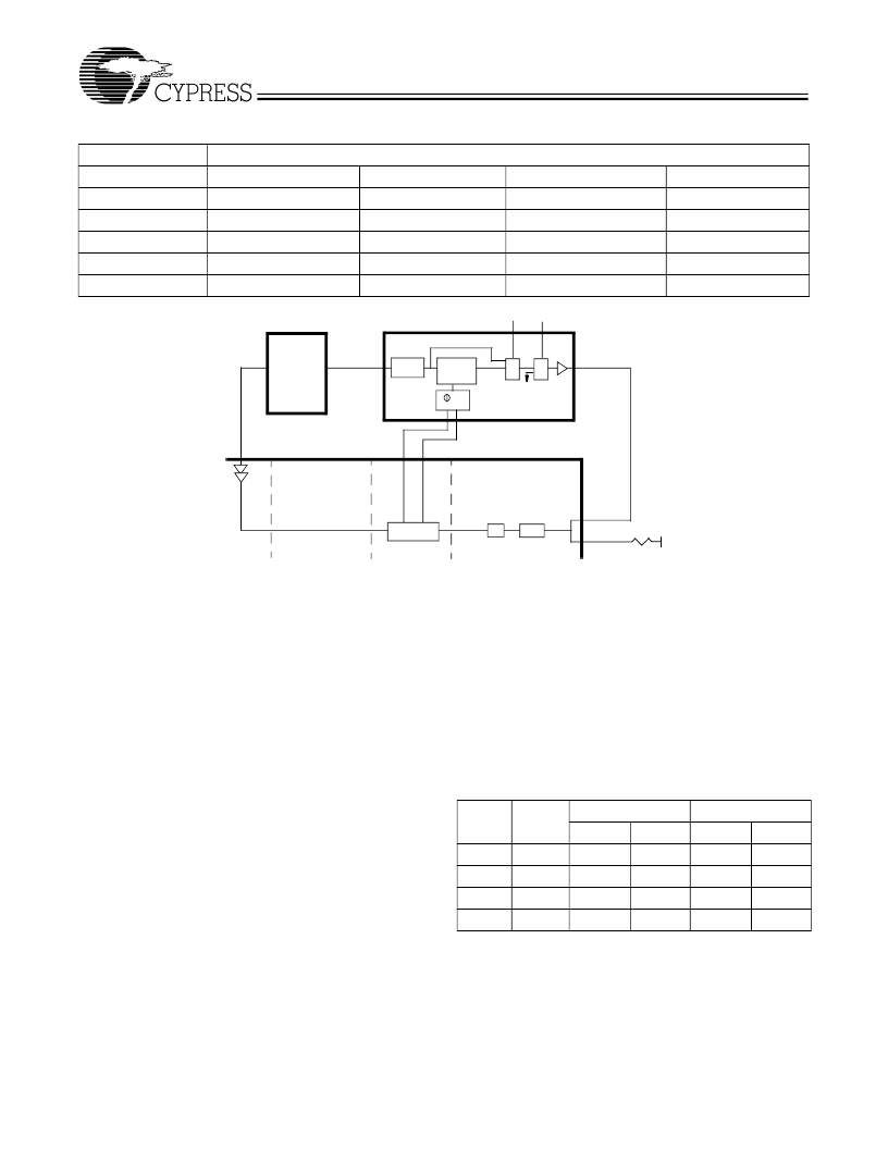
Figure 3
shows more details of the DDLL system architecture,
including the DRCG output enable and bypass modes.
Phase Detector Signals
The DRCG Phase Detector receives two inputs from the core
logic, PclkM (Pclk/M) and SynclkN (Synclk/N). The M and N
dividers in the core logic are chosen so that the frequencies of
PclkM and SynclkN are identical. The Phase Detector detects
the phase difference between the two input clocks, and drives
the DRCG Phase Aligner to null the input phase error through
the distributed loop. When the loop is locked, the input phase
error between PclkM and SynclkN is within the specification
t
ERR,PD
given in
Table 14
after the lock time given in the State
Transition Section.
The Phase Detector aligns the rising edge of PclkM to the
rising edge of SynclkN. The duty cycle of the phase detector
input clocks will be within the specification DC
IN,PD
given in
Table 13
. Because the duty cycles of the two phase detector
input clocks will not necessarily be identical, the falling edges
of PclkM and SynclkN may not be aligned when the rising edg-
es are aligned.
The voltage levels of the PclkM and SynclkN signals are de-
termined by the controller. The pin VDDIPD is used as the
voltage reference for the phase detector inputs and should be
connected to the output voltage supply of the controller. In
some applications, the DRCG PLL output clock will be used
directly, by bypassing the Phase Aligner. If PclkM and SynclkN
are not used, those inputs must be grounded.
Selection Logic
Table 2
shows the logic for selecting the PLL prescaler and
feedback dividers to determine the multiply ratio for the PLL
from the input Refclk. Divider A sets the feedback and divider
B sets the prescaler, so the PLL output clock frequency is set
by: PLLclk=Refclk*A/B.
Table 3
shows the logic for enabling the clock outputs, using
the StopB input signal. When StopB is HIGH, the DRCG is in
its normal mode, and Clk and ClkB are complementary outputs
following the Phase Aligner output (PAclk). When StopB is
LOW, the DRCG is in the Clk Stop mode, the output clock
drivers are disabled (set to Hi-Z), and the Clk and ClkB settle
to the DC voltage V
X,STOP
as given in
Table 14
. The level of
V
X,STOP
is set by an external resistor network.
Table 1. Supported Pclk and Busclk Frequencies, by Gear Ratio
Gear Ratio and Busclk
1.5
Pclk
2.0
1.33
1.0
67 MHz
100 MHz
133 MHz
150 MHz
200 MHz
267 MHz
400 MHz
300 MHz
400 MHz
267 MHz
356 MHz
400 MHz
400 MHz
W134M/W134S
Refclk
W133
W158
W159
W161
W167
CY2210
PLL
Phase
Align
D
4
DLL
RAC
RMC
M N
Gear
Ratio
Logic
Pclk
Busclk
Synclk
P
S
S0/S1 StopB
Figure 3. DDLL Including Details of DRCG
Table 2. PLL Divider Selection
Mult0
0
0
1
1
Mult1
0
1
1
0
W134M
W134S
A
9
6
8
16
B
2
1
1
3
A
4
6
8
16
B
1
1
1
3
相关PDF资料 |
PDF描述 |
|---|---|
| W132-10B | Ten Distributed-Output Clock Driver |
| W132-10BX | Ten Distributed-Output Clock Driver |
| W132-09B | Nine Distributed-Output Clock Driver |
| W134MH | Miscellaneous Clock Generator |
| W134M | Direct Rambus Clock Generator |
相关代理商/技术参数 |
参数描述 |
|---|---|
| W132-09BXT | 制造商:Cypress Semiconductor 功能描述:SPREAD AWARE ZERO DELAY BUFFER |
| W132-10B | 制造商:未知厂家 制造商全称:未知厂家 功能描述:Ten Distributed-Output Clock Driver |
| W132-10BX | 制造商:Cypress Semiconductor 功能描述:Zero Delay PLL Clock Buffer Single 25MHz to 140MHz 24-Pin TSSOP 制造商:Rochester Electronics LLC 功能描述:- Bulk |
| W132-10BXT | 制造商:Cypress Semiconductor 功能描述:Zero Delay PLL Clock Buffer Single 25MHz to 140MHz 24-Pin TSSOP T/R 制造商:Rochester Electronics LLC 功能描述:CLK DRIVER - Tape and Reel |
| W132E13B | 制造商:OMRON INDUSTRIAL AUTOMATION 功能描述:Discontinued |
发布紧急采购,3分钟左右您将得到回复。