- 您现在的位置:买卖IC网 > PDF目录361766 > W185-5 (Cypress Semiconductor Corp.) Six Output Peak Reducing EMI Solution PDF资料下载
参数资料
| 型号: | W185-5 |
| 厂商: | Cypress Semiconductor Corp. |
| 英文描述: | Six Output Peak Reducing EMI Solution |
| 中文描述: | 六输出峰值抑制EMI解决方案 |
| 文件页数: | 2/8页 |
| 文件大小: | 116K |
| 代理商: | W185-5 |
W185
2
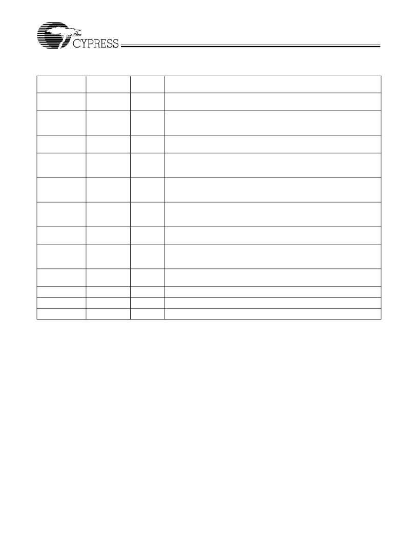
Pin Definitions
Pin Name
Pin No.
Pin
Type
Pin Description
CLK0:5
9, 11, 12, 13,
15, 17
O
Modulated Frequency Outputs:
Frequency modulated copies of the unmod-
ulated input clock (SSON# asserted).
CLKIN or X1
3
I
Crystal Connection or External Reference Frequency Input:
This pin has
dual functions. It may either be connected to an external crystal, or to an
external reference clock.
NC or X2
4
I
Crystal Connection:
If using an external reference, this pin must be left un-
connected.
SS%
6
I
Modulation Width Selection:
When Spread Spectrum feature is turned on,
this pin is used to select the amount of variation and peak EMI reduction that
is desired on the output signal. This pin has an internal pull-up resistor.
Reset
23
I
Modulation Profile Restart:
A rising edge on this input restarts the modulation
pattern at the beginning of its defined path. This pin has an internal pull-down
resistor.
REFOUT
1
O
Non-Modulated Output:
This pin provides a copy of the reference frequency.
This output will not have the Spread Spectrum feature enabled regardless of
the state of logic input SSON#.
EN1:2
18, 7
I
Output Enable Select Pins:
These pins control the activity of specific output
buffers. See
Table 3
on page 1.
SSON#
24
I
Spread Spectrum Control (Active LOW):
Asserting this signal (active LOW)
turns the internal modulation waveform on. This pin has an internal pull-down
resistor.
FS1:2
22, 2
I
Frequency Selection Bit 1 and 2:
These pins select the frequency of opera-
tion. Refer to
Table 1
. These pins have internal pull-up resistors.
VDD
10, 16, 20, 21
P
Power Connection:
Connected to 3.3V or 5V power supply.
GND
5, 8, 14
G
Ground Connection:
This should be connected to the common ground plane.
NC
19
NC
No Connect:
This pin should be left floating.
相关PDF资料 |
PDF描述 |
|---|---|
| W18NB40 | N-CHANNEL 400V - 0.19ohm - 18.4A TO-247/ISOWATT218 PowerMESH MOSFET |
| W191 | Clocks and Buffers |
| W194-70G | Miscellaneous Clock Generator |
| W195 | Clocks and Buffers |
| W2005ABE | FM Receiver Circuit |
相关代理商/技术参数 |
参数描述 |
|---|---|
| W185-5H | 制造商:Rochester Electronics LLC 功能描述:TIMING DEVICE - Bulk |
| W185-5HI | 制造商:Rochester Electronics LLC 功能描述:- Bulk |
| W185E11 | 制造商:OMRON INDUSTRIAL AUTOMATION 功能描述:HIGH-SPEED COUNTER UNIT -CT041 DX CODE ZA |
| W185H | 制造商:未知厂家 制造商全称:未知厂家 功能描述:Miscellaneous Clock Generator |
| W185HT | 制造商:Cypress Semiconductor 功能描述: |
发布紧急采购,3分钟左右您将得到回复。