- 您现在的位置:买卖IC网 > PDF目录361766 > W195 Clocks and Buffers PDF资料下载
参数资料
| 型号: | W195 |
| 英文描述: | Clocks and Buffers |
| 中文描述: | 时钟和缓冲器 |
| 文件页数: | 2/14页 |
| 文件大小: | 142K |
| 代理商: | W195 |
W195B
PRELIMINARY
Document #: 38-07160 Rev. *A
Page 2 of 14
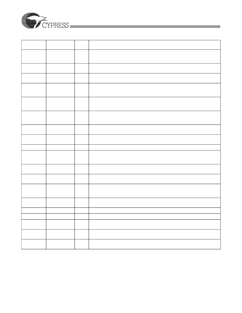
Pin Definitions
Pin Name
REF2x/FS3
Pin No.
1
Pin
Type
I/O
Pin Description
Reference Clock with 2x Drive/Frequency Select 3:
3.3V 14.318-MHz clock out-
put. This pin also serves as the select strap to determine device operating frequency
as described in
Table 1
.
Crystal Input:
This pin has dual functions. It can be used as an external 14.318-
MHz crystal connection or as an external reference frequency input.
Crystal Output:
An input connection for an external 14.318-MHz crystal connec-
tion. If using an external reference, this pin must be left unconnected.
PCI Clock 0/Frequency Selection 0:
3.3V 33-MHz PCI clock outputs. This pin also
serves as the select strap to determine device operating frequency as described in
Table 1
.
PCI Clock 1/Frequency Selection 1:
3.3V 33-MHz PCI clock outputs. This pin also
serves as the select strap to determine device operating frequency as described in
Table 1
.
PCI Clock 2/Frequency Selection 2:
3.3V 33-MHz PCI clock outputs. This pin
doubles as the select strap to determine device operating frequency as described
in
Table 1
.
PCI Clock 3 through 7:
3.3V 33-MHz PCI clock outputs. PCI0:7 can be individually
turned off via I
2
C interface.
66-MHz Clock Output:
3.3V output clocks. The operating frequency is controlled
by FS0:3 (see
Table 1
).
48-MHz Clock Output
: 3.3V fixed 48-MHz, non-spread spectrum clock output.
Clock Output for Super I/O:
This is the input clock for a Super I/O (SIO) device.
During power-up, it also serves as a selection strap. If it is sampled HIGH, the output
frequency for SIO is 24 MHz. If the input is sampled LOW, the output is 48 MHz.
Power Down Control:
LVTTL-compatible input that places the device in power-
down mode when held LOW.
CPU Clock Outputs:
Clock outputs for the host bus interface. Output frequencies
depending on the configuration of FS0:3. Voltage swing is set by V
DDQ2
.
SDRAM Clock Outputs:
3.3V outputs for SDRAM. The operating frequency is
controlled by FS0:3 (see
Table 1
).
X1
3
I
X2
4
I
PCI0/FS0
10
I/O
PCI1/FS1
11
I/O
PCI2/FS2
12
I/O
PCI3:7
14, 15, 17, 18,
19
7,8
O
3V66_0:1
O
48MHz_0:1
SIO/
24_48#MHz
21, 22
23
O
I/O
PWRDWN#
29
I
CPU0:1
45, 44
O
SDRAM0:8,
41, 40, 39, 37,
36, 35, 33, 32,
31
47
O
APIC
O
Synchronous APIC Clock Outputs:
Clock outputs running synchronous with the
PCI clock outputs. Voltage swing set by V
DDQ2
.
Data pin for I
2
C circuitry.
Clock pin for I
2
C circuitry.
3.3V Power Connection:
Power supply for SDRAM output buffers, PCI output buff-
ers, reference output buffers, and 48-MHz output buffers. Connect to 3.3V.
2.5V Power Connection:
Power supply for IOAPIC and CPU output buffers. Con-
nect to 2.5V or 3.3V.
Ground Connections:
Connect all ground pins to the common system ground
plane.
SDATA
SCLK
VDDQ3
25
28
I/O
I
P
2, 6, 16, 24, 27,
34, 42
46, 48
VDDQ2
P
GND
5, 9, 13, 20, 26,
30, 38, 43
G
相关PDF资料 |
PDF描述 |
|---|---|
| W2005ABE | FM Receiver Circuit |
| W2005BBE | FM Receiver Circuit |
| W2010AAF | RF Modulator |
| W2011 | RF Modulator |
| W2011BBY | RF Modulator |
相关代理商/技术参数 |
参数描述 |
|---|---|
| W195B | 制造商:CYPRESS 制造商全称:Cypress Semiconductor 功能描述:Frequency Generator for Integrated Core Logic |
| W195E15 | 制造商:Omron Corporation 功能描述: |
| W195E33 | 制造商:OMRON INDUSTRIAL AUTOMATION 功能描述:CV Series Install. |
| W196 | 制造商:CYPRESS 制造商全称:Cypress Semiconductor 功能描述:Spread Spectrum FTG for 440BX and VIA Apollo Pro-133 |
| W196_02 | 制造商:CYPRESS 制造商全称:Cypress Semiconductor 功能描述:Spread Spectrum FTG for 440BX and VIA Apollo Pro-133 |
发布紧急采购,3分钟左右您将得到回复。