- 您现在的位置:买卖IC网 > PDF目录361766 > W195 Clocks and Buffers PDF资料下载
参数资料
| 型号: | W195 |
| 英文描述: | Clocks and Buffers |
| 中文描述: | 时钟和缓冲器 |
| 文件页数: | 6/14页 |
| 文件大小: | 142K |
| 代理商: | W195 |
W195B
PRELIMINARY
Document #: 38-07160 Rev. *A
Page 6 of 14
Serial Data Interface
The W195B features a two-pin, serial data interface that can
be used to configure internal register settings that control par-
ticular device functions.
Data Protocol
The clock driver serial protocol accepts only block writes from
the controller. The bytes must be accessed in sequential order
from lowest to highest byte with the ability to stop after any
complete byte has been transferred. Indexed bytes are not
allowed.
A block write begins with a slave address and a write condition.
After the command code the core logic issues a byte count
which describes how many more bytes will follow in the mes-
sage. If the host had 20 bytes to send. The first byte would be
the number 20 (14h), followed by the 20 bytes of data. The
byte count may not be 0. A block write command is allowed to
transfer a maximum of 32 data bytes. The slave receiver ad-
dress for W195B is 11010010.
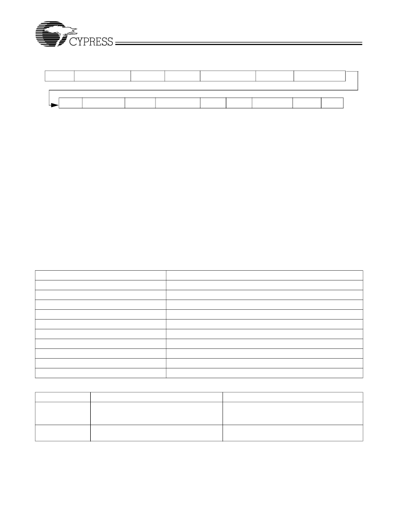
Figure 7
shows an example of
a block write.
The command code and the byte count bytes are required as
the first two bytes of any transfer. W195B expects a command
code of 0000 0000. The byte count byte is the number of ad-
ditional bytes required for the transfer, not counting the com-
mand code and byte count bytes. Additionally, the byte count
byte is required to be a minimum of 1 byte and a maximum of
32 bytes to satisfy the above requirement.
Table 2
shows an
example of a possible byte count value.
A transfer is considered valid after the acknowledge bit corre-
sponding to the byte count is read by the controller. The com-
mand code and byte count bytes are ignored by the W195B.
However, these bytes must be included in the data write se-
quence to maintain proper byte allocation.
Notes:
6.
7.
The acknowledgment bit is returned by the slave/receiver (W195B).
Byte 6 and 7 are not defined for W195B.
1 bit
7 bits
1
1
8 bits
1
Start bit
Slave Address
R/W
Ack
Command Code
Ack
Byte Count = N
Ack
Data Byte 1
Ack
Data Byte 2
Ack
...
Data Byte N
Ack
Stop
1 bit
8 bits
1
8 bits
1
8 bits
1
1
Figure 7. An Example of a Block Write
[6]
Table 2. Example of Possible Byte Count Value
Byte Count Byte
MSB
0000
0000
0000
0000
0000
0000
0000
0000
0010
Notes
LSB
0000
0001
0010
0011
0100
0101
0110
0111
0000
Not allowed. Must have at least one byte.
Data for functional and frequency select register (currently byte 0 in spec)
Reads first two bytes of data. (byte 0 then byte 1)
Reads first three bytes (byte 0, 1, 2 in order)
Reads first four bytes (byte 0, 1, 2, 3 in order)
Reads first five bytes (byte 0, 1, 2, 3, 4 in order)
[7]
Reads first six bytes (byte 0, 1, 2, 3, 4, 5 in order)
[7]
Reads first seven bytes (byte 0, 1, 2, 3, 4, 5, 6 in order)
Max. byte count supported = 32
Table 3. Serial Data Interface Control Functions Summary
Control Function
Output Disable
Any individual clock output(s) can be disabled.
Disabled outputs are actively held LOW.
Description
Common Application
Unused outputs are disabled to reduce EMI and sys-
tem power. Examples are clock outputs to unused
PCI slots.
No user application. Register bit must be written as 0.
(Reserved)
Reserved function for future device revision or pro-
duction device testing.
相关PDF资料 |
PDF描述 |
|---|---|
| W2005ABE | FM Receiver Circuit |
| W2005BBE | FM Receiver Circuit |
| W2010AAF | RF Modulator |
| W2011 | RF Modulator |
| W2011BBY | RF Modulator |
相关代理商/技术参数 |
参数描述 |
|---|---|
| W195B | 制造商:CYPRESS 制造商全称:Cypress Semiconductor 功能描述:Frequency Generator for Integrated Core Logic |
| W195E15 | 制造商:Omron Corporation 功能描述: |
| W195E33 | 制造商:OMRON INDUSTRIAL AUTOMATION 功能描述:CV Series Install. |
| W196 | 制造商:CYPRESS 制造商全称:Cypress Semiconductor 功能描述:Spread Spectrum FTG for 440BX and VIA Apollo Pro-133 |
| W196_02 | 制造商:CYPRESS 制造商全称:Cypress Semiconductor 功能描述:Spread Spectrum FTG for 440BX and VIA Apollo Pro-133 |
发布紧急采购,3分钟左右您将得到回复。