- 您现在的位置:买卖IC网 > PDF目录221598 > W3E16M72S-250BC (WHITE ELECTRONIC DESIGNS CORP) 16M X 72 DDR DRAM, 0.8 ns, PBGA219 PDF资料下载
参数资料
| 型号: | W3E16M72S-250BC |
| 厂商: | WHITE ELECTRONIC DESIGNS CORP |
| 元件分类: | DRAM |
| 英文描述: | 16M X 72 DDR DRAM, 0.8 ns, PBGA219 |
| 封装: | 32 X 25 MM, PLASTIC, BGA-219 |
| 文件页数: | 16/17页 |
| 文件大小: | 766K |
| 代理商: | W3E16M72S-250BC |
8
White Electronic Designs Corporation (602) 437-1520 www.whiteedc.com
White Electronic Designs
W3E16M72S-XBX
February 2005
Rev. 7
selects the starting column location. The value on input A10
determines whether or not AUTO PRECHARGE is used. If
AUTO PRECHARGE is selected, the row being accessed
will be precharged at the end of the WRITE burst; if AUTO
PRECHARGE is not selected, the row will remain open for
subsequent accesses. Input data appearing on the D/Qs is
written to the memory array subject to the DQM input logic
level appearing coincident with the data. If a given DQM
signal is registered LOW, the corresponding data will be
written to memory; if the DQM signal is registered HIGH,
the corresponding data inputs will be ignored, and a WRITE
will not be executed to that byte/column location.
PRECHARGE
The PRECHARGE command is used to deactivate the
open row in a particular bank or the open row in all banks.
The bank(s) will be available for a subsequent row access
a specied time (tRP) after the PRECHARGE command is
issued. Except in the case of concurrent auto precharge,
where a READ or WRITE command to a different bank is
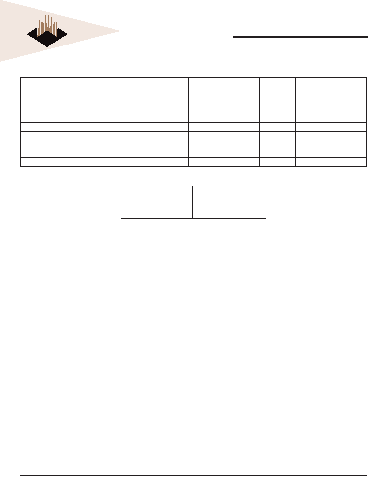
TRUTH TABLE – COMMANDS (NOTE 1)
NAME (FUNCTION)
CS#
RAS#
CAS#
WE#
ADDR
DESELECT (NOP) (9)
H
X
NO OPERATION (NOP) (9)
L
H
X
ACTIVE (Select bank and activate row) ( 3)
L
H
Bank/Row
READ (Select bank and column, and start READ burst) (4)
L
H
L
H
Bank/Col
WRITE (Select bank and column, and start WRITE burst) (4)
L
H
L
Bank/Col
BURST TERMINATE (8)
L
H
L
X
PRECHARGE (Deactivate row in bank or banks) ( 5)
L
H
L
Code
AUTO REFRESH or SELF REFRESH (Enter self refresh mode) (6, 7)
L
H
X
LOAD MODE REGISTER (2)
L
Op-Code
NOTES:
1. CKE is HIGH for all commands shown except SELF REFRESH.
2. A0-12 dene the op-code to be written to the selected Mode Register. BA0, BA1
select either the mode register (0, 0) or the extended mode register (1, 0).
3. A0-12 provide row address, and BA0, BA1 provide bank address.
4. A0-8 provide column address; A10 HIGH enables the auto precharge feature (non
persistent), while A10 LOW disables the auto precharge feature; BA0, BA1 provide
bank address.
5. A10 LOW: BA0, BA1 determine the bank being precharged. A10 HIGH: All banks
precharged and BA0, BA1 are “Don’t Care.”
6. This command is AUTO REFRESH if CKE is HIGH; SELF REFRESH if CKE is LOW.
7. Internal refresh counter controls row addressing; all inputs and I/Os are “Don’t Care”
except for CKE.
8. Applies only to read bursts with auto precharge disabled; this command is undened
(and should not be used) for READ bursts with auto precharge enabled and for
WRITE bursts.
9. DESELECT and NOP are functionally interchangeable.
10. Used to mask write data; provided coincident with the corresponding data.
on inputs A0-12 selects the row. This row remains active
(or open) for accesses until a PRECHARGE command is
issued to that bank. A PRECHARGE command must be
issued before opening a different row in the same bank.
READ
The READ command is used to initiate a burst read access
to an active row. The value on the BA0, BA1 inputs selects
the bank, and the address provided on inputs A0-8 selects
the starting column location. The value on input A10
determines whether or not AUTO PRECHARGE is used. If
AUTO PRECHARGE is selected, the row being accessed
will be precharged at the end of the READ burst; if AUTO
PRECHARGE is not selected, the row will remain open for
subsequent accesses.
WRITE
The WRITE command is used to initiate a burst write
access to an active row. The value on the BA0, BA1 inputs
selects the bank, and the address provided on inputs A0-8
TRUTH TABLE – DM OPERATION
NAME (FUNCTION)
DM
DQs
WRITE ENABLE (10)
L
Valid
WRITE INHIBIT (10)
H
X
相关PDF资料 |
PDF描述 |
|---|---|
| WV3HG64M72EER665D7MG | 64M X 72 DDR DRAM MODULE, DMA244 |
| WPS256K16B-17LJCGA | 256K X 16 STANDARD SRAM, 17 ns, PDSO44 |
| WS57C010F-25E | 128K X 8 OTPROM, 25 ns, PDSO32 |
| WS57C010F-45CI | 128K X 8 UVPROM, 45 ns, CQCC32 |
| WF512K64-90G4WI5A | 4M X 8 FLASH 5V PROM MODULE, 90 ns, CQMA116 |
相关代理商/技术参数 |
参数描述 |
|---|---|
| W3E16M72S-250BI | 制造商:Microsemi Corporation 功能描述:16M X 72 DDR, 2.5V, 250 MHZ, 219 PBGA, INDUSTRIAL TEMP. - Bulk |
| W3E16M72S-250BM | 制造商:Microsemi Corporation 功能描述:16M X 72 DDR, 2.5V, 250 MHZ, 219 PBGA, MIL-TEMP. - Bulk |
| W3E16M72S-266BC | 制造商:Microsemi Corporation 功能描述:16M X 72 DDR, 2.5V, 266 MHZ, 219 PBGA, COMMERCIAL TEMP. - Bulk |
| W3E16M72S-266BI | 制造商:Microsemi Corporation 功能描述:16M X 72 DDR, 2.5V, 266 MHZ, 219 PBGA, INDUSTRIAL TEMP. - Bulk |
| W3E16M72S-266BM | 制造商:Microsemi Corporation 功能描述:16M X 72 DDR, 2.5V, 266 MHZ, 219 PBGA, MIL-TEMP. - Bulk |
发布紧急采购,3分钟左右您将得到回复。