- 您现在的位置:买卖IC网 > PDF目录276891 > W3E32M64SA-200BI (MICROSEMI CORP-PMG MICROELECTRONICS) 32M X 64 DDR DRAM, 0.8 ns, PBGA219 PDF资料下载
参数资料
| 型号: | W3E32M64SA-200BI |
| 厂商: | MICROSEMI CORP-PMG MICROELECTRONICS |
| 元件分类: | DRAM |
| 英文描述: | 32M X 64 DDR DRAM, 0.8 ns, PBGA219 |
| 封装: | 25 X 25 MM, PLASTIC, BGA-219 |
| 文件页数: | 6/17页 |
| 文件大小: | 701K |
| 代理商: | W3E32M64SA-200BI |
W3E32M64SA-XBX
14
White Electronic Designs Corporation (602) 437-1520 www.whiteedc.com
White Electronic Designs
December 2007
Rev. 1
28. To maintain a valid level, the transitioning edge of the input must:
a) Sustain a constant slew rate from the current AC level through to the target AC
level, VIL(AC) or VIH(AC).
b) Reach at least the target AC level.
c) After the AC target level is reached, continue to maintain at least the target DC
level, VIL(DC) or VIH(DC).
29. The Input capacitance per pin group will not differ by more than this maximum
amount for any given device.
30. CK and CK# input slew rate must be > 1V/ns (>2V/ns differentially).
31. DQ and DM input slew rates must not deviate from DQS by more than 10%. If the
DQ/DM/DQS slew rate is less than 0.5V/ns, timing must be derated: 50ps must be
added to tDS and tDH for each 100mV/ns reduction in slew rate. If slew rate exceeds
4V/ns, functionality is uncertain.
32. VCC must not vary more than 4% if CKE is not active while any bank is active.
33. The clock is allowed up to ±150ps of jitter. Each timing parameter is allowed to vary
by the same amount.
34. tHP min is the lesser of tCL minimum and tCH minimum actually applied to the device
CK and CK# inputs, collectively during bank active.
35. READs and WRITEs with auto precharge are not allowed to be issued until
tRAS(MIN) can be satised prior to the internal precharge command being issued.
36. Any positive glitch must be less than 1/3 of the clock and not more than +400mV or
2.9 volts, whichever is less. Any negative glitch must be less than
1/3 of the clock cycle and not exceed either -300mV or 2.2 volts, whichever is more
positive. The average cannot be below the 2.5V minimum.
37. Normal Output Drive Curves:
a) The full variation in driver pull-down current from minimum to maximum
process, temperature and voltage will lie within the outer bounding lines of the
V-I curve of Figure A.
b) The variation in driver pull-down current within nominal limits of voltage and
temperature is expected, but not guaranteed, to lie within the inner bounding
lines of the V-I curve of Figure A.
c) The full variation in driver pull-up current from minimum to maximum process,
temperature and voltage will lie within the outer bounding lines of the V-I curve
of Figure B.
d) The variation in driver pull-up current within nominal limits of voltage and
temperature is expected, but not guaranteed, to lie within the inner bounding
lines of the V-I curve of Figure B.
e) The full variation in the ratio of the maximum to minimum pull-up and pull-down
current should be between .71 and 1.4, for device drain-to-source voltages from
0.1V to 1.0 Volt, and at the same voltage and temperature.
f) The full variation in the ratio of the nominal pull-up to pull-down current should
be unity ±10%, for device drain-to-source voltages from 0.1V to 1.0 Volt.
38. Reduced Output Drive Curves:
a) The full variation in driver pull-down current from minimum to maximum
process, temperature and voltage will lie within the outer bounding lines of the
V-I curve of Figure C.
b) The variation in driver pull-down current within nominal limits of voltage and
temperature is expected, but not guaranteed, to lie within the inner bounding
lines of the V-I curve of Figure C.
c) The full variation in driver pull-up current from minimum to maximum process,
temperature and voltage will lie within the outer bounding lines of the V-I curve
of Figure D.
d) The variation in driver pull-up current within nominal limits of voltage and
temperature is expected, but not guaranteed, to lie within the inner bounding
lines of the V-I curve of Figure D.
e) The full variation in the ratio of the maximum to minimum pull-up and pull-down
current should be between .71 and 1.4, for device drain-to-source voltages from
0.1V to 1.0 V, and at the same voltage and temperature.
f) The full variation in the ratio of the nominal pull-up to pull-down current should
be unity ±10%, for device drain-to-source voltages from 0.1V to 1.0 V.
39. The voltage levels used are derived from a minimum VCC level and the referenced
test load. In practice, the voltage levels obtained from a properly terminated bus will
provide signicantly different voltage values.
40. VIH overshoot: VIH(MAX) = VCCQ+1.5V for a pulse width < 3ns and the pulse width
can not be greater than 1/3 of the cycle rate. VIL undershoot: VIL (MIN) = -1.5V for a
pulse width < 3ns and the pulse width cannot be greater than 1/3 of the cycle rate.
41. VCC and VCCQ must track each other.
42. tHZ (MAX) will prevail over tDQSCK (MAX) + tRPST (MAX) condition. tLZ (MIN) will
prevail over tDQSCK (MIN) + tRPRE (MAX) condition.
43. tRPST end point and tRPRE begin point are not referenced to a specic voltage level
but specify when the device output is no longer driving (tRPST), or begins driving
(tRPRE).
44. During initialization, VCCQ, VTT, and VREF must be equal to or less than VCC + 0.3V.
Alternatively, VTT may be 1.35V maximum during power up, even if VCC/VCCQ are 0
volts, provided a minimum of 42 ohms of series resistance is used between the VTT
supply and the input pin.
45. The current part operates below the slowest JEDEC operating frequency of 83 MHz.
As such, future die may not reect this option.
46. When an input signal is HIGH or LOW, it is dened as a steady state logic HIGH or
LOW.
47. Random addressing changing 50% of data changing at every transfer.
48. Random addressing changing 100% of data changing at every transfer.
49.. CKE must be active (high) during the entire time a refresh command is executed.
That is, from the time the AUTO REFRESH command is registered, CKE must be
active at each rising clock edge, until tRFC has been satised.
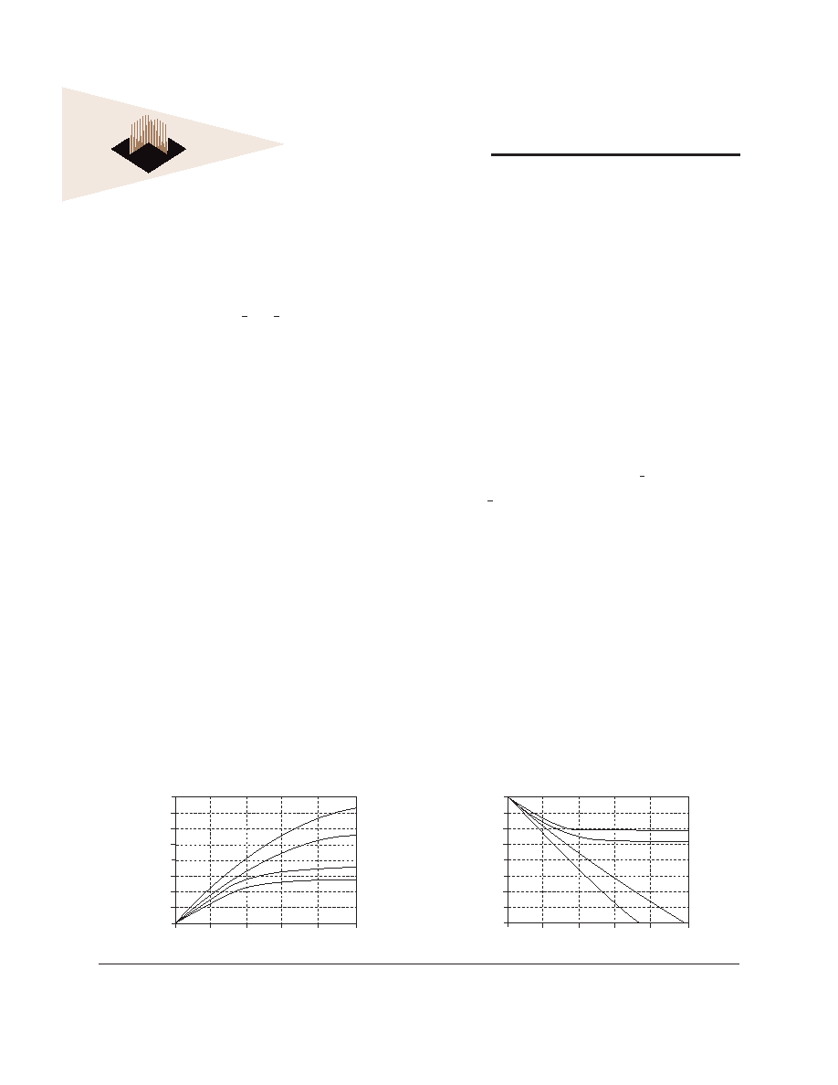
FIGURE C – PULL-DOWN CHARACTERISTICS
80
70
60
50
40
30
20
10
0
0.0
0.5
1.0
1.5
2.0
2.5
VOUT (V)
IOUT
(mA)
Maximum
Nominal high
Nominal low
Minimum
FIGURE D – PULL-UP CHARACTERISTICS
0.0
0.5
1.0
1.5
2.0
2.5
VCCQ - VOUT (V)
IOUT
(mA)
Maximum
Nominal high
Nominal low
Minimum
0
-10
-20
-30
-40
-50
-60
-70
-80
相关PDF资料 |
PDF描述 |
|---|---|
| W3EG72256S265JD3MF | 256M X 72 DDR DRAM MODULE, 0.75 ns, DMA184 |
| W3EG7232S202AD4S | 32M X 72 DDR DRAM MODULE, 0.75 ns, DMA200 |
| W3EG7232S202BD4IMG | 32M X 72 DDR DRAM MODULE, 0.75 ns, DMA200 |
| W3EG7232S262AD4ISG | 32M X 72 DDR DRAM MODULE, 0.75 ns, DMA200 |
| W3EG7232S265BD4SG | 32M X 72 DDR DRAM MODULE, 0.75 ns, DMA200 |
相关代理商/技术参数 |
参数描述 |
|---|---|
| W3E32M64SA-200BM | 制造商:Microsemi Corporation 功能描述:32M X 64 DDR, 2.5V, 200 MHZ, 219 PBGA, MIL-TEMP. - Bulk |
| W3E32M64SA-250BC | 制造商:Microsemi Corporation 功能描述:32M X 64 DDR, 2.5V, 250 MHZ, 219 PBGA, COMMERCIAL TEMP. - Bulk |
| W3E32M64SA-250BI | 制造商:Microsemi Corporation 功能描述:32M X 64 DDR, 2.5V, 250 MHZ, 219 PBGA, INDUSTRIAL TEMP. - Bulk |
| W3E32M64SA-250BM | 制造商:Microsemi Corporation 功能描述:32M X 64 DDR, 2.5V, 250 MHZ, 219 PBGA, MIL-TEMP. - Bulk |
| W3E32M64SA-266BC | 制造商:Microsemi Corporation 功能描述:32M X 64 DDR, 2.5V, 266 MHZ, 219 PBGA, COMMERCIAL TEMP. - Bulk |
发布紧急采购,3分钟左右您将得到回复。