- 您现在的位置:买卖IC网 > PDF目录68457 > W3H32M64EA-667SBC (MICROSEMI CORP-PMG MICROELECTRONICS) 32M X 64 DDR DRAM, PBGA208 PDF资料下载
参数资料
| 型号: | W3H32M64EA-667SBC |
| 厂商: | MICROSEMI CORP-PMG MICROELECTRONICS |
| 元件分类: | DRAM |
| 英文描述: | 32M X 64 DDR DRAM, PBGA208 |
| 封装: | 16 X 20 MM, 1 MM PITCH, PLASTIC, BGA-208 |
| 文件页数: | 14/28页 |
| 文件大小: | 1057K |
| 代理商: | W3H32M64EA-667SBC |
第1页第2页第3页第4页第5页第6页第7页第8页第9页第10页第11页第12页第13页当前第14页第15页第16页第17页第18页第19页第20页第21页第22页第23页第24页第25页第26页第27页第28页
21
White Electronic Designs Corporation (602) 437-1520 www.whiteedc.com
White Electronic Designs
February 2010 2010 White Electronic Designs Corp. All rights reserved
Rev. 0
ADVANCED
White Electronic Designs Corp. reserves the right to change products or specications without notice.
W3H32M64EA-XSBX
21
White Electronic Designs Corporation (602) 437-1520 www.whiteedc.com
White Electronic Designs
February 2010 2010 White Electronic Designs Corp. All rights reserved
Rev. 0
ADVANCED
White Electronic Designs Corp. reserves the right to change products or specications without notice.
W3H32M64EA-XSBX
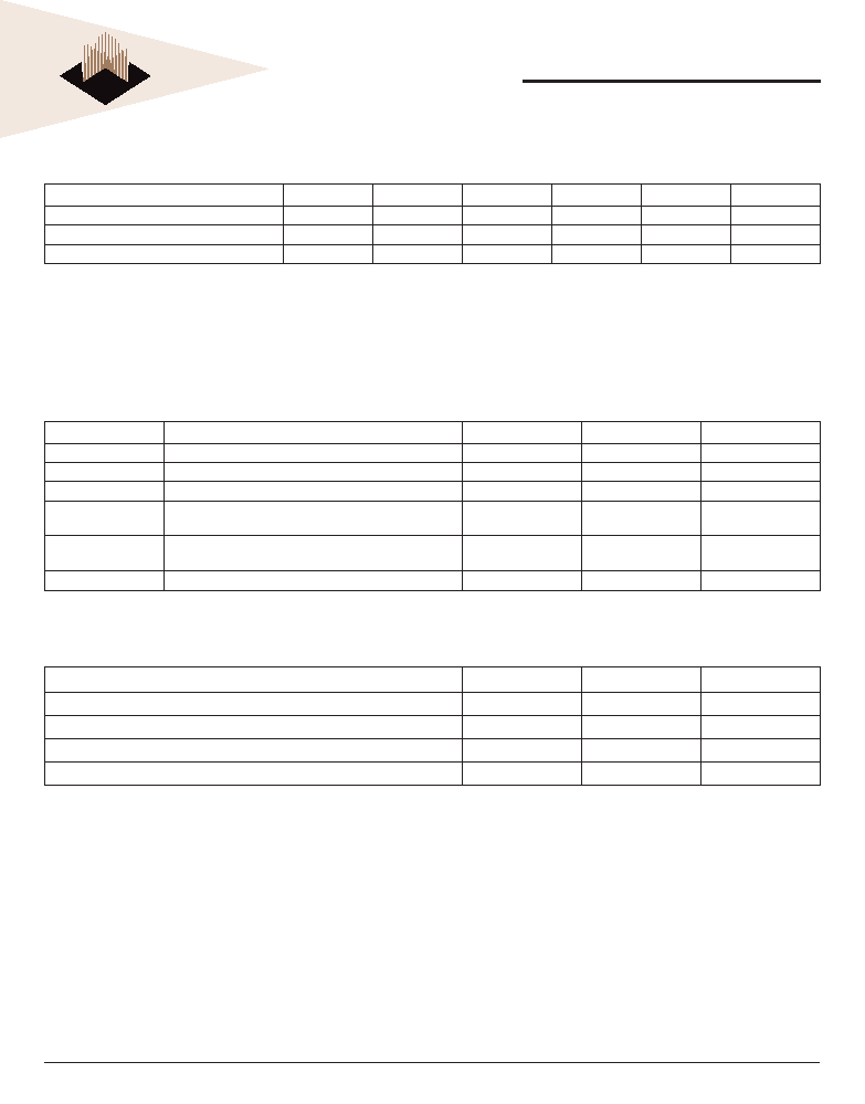
DC OPERATING CONDITIONS
All voltages referenced to VSS
Parameter
Symbol
Min
Typical
Max
Unit
Notes
Supply voltage
VCC
1 .7
1 .8
1 .9
V
1
I/O Reference voltage
VREF
0.49 x VCCQ
0.50 x VCCQ
0.51 x VCCQ
V2
I/O Termination voltage
VTT
VREF-0.04
VREF
VREF + 0.04
V
3
Notes:
1.
VCC and VCCQ are tied on the device.
2.
VREF is expected to equal VCCQ/2 of the transmitting device and to track variations in the DC level of the same. Peak-to-peak noise on VREF may not exceed ±1 percent of the DC
value. Peak-to-peak AC noise on VREF may not exceed ±2 percent of VREF. This measurement is to be taken at the nearest VREF bypass capacitor.
3.
VTT is not applied directly to the device. VTT is a system supply for signal termination resistors, is expected to be set equal to VREF and must track variations in the DC level of VREF.
ABSOLUTE MAXIMUM RATINGS
Symbol
Parameter
MIN
MAX
U nit
VCC/ VCCQ
Voltage on VCC pin relative to VSS
-0.5
2.3
V
VIN, VOUT
Voltage on any pin relative to VSS
-0.5
2.3
V
TSTG
Storage temperature
-55
125
°C
IL
Input leakage current; Any input 0V<VIN<VCC; Other pins
not under test = 0V
-20
20
μA
IOZ
Output leakage current;
0V<VOUT<VCC; DQs and ODT are disabled
-5
5
μA
IVREF
VREF leakage current; VREF = Valid VREF level
-8
8
μA
INPUT/OUTPUT CAPACITANCE
TA = 25°C, f = 1MHz, VCC = 1.8V
Parameter
Symbol
Max
Unit
Input capacitance (A0 - A13, BA0 - BA2 ,CS#, RAS#,CAS#,WE#, CKE, ODT)
CIN1
TBD
pF
Input capacitance CK, CK#
CIN2
TBD
pF
Input capacitance DM, DQS, DQS#
CIN3
TBD
pF
Input capacitance DQ0 - 63
COUT
TBD
pF
相关PDF资料 |
PDF描述 |
|---|---|
| W3H32M72E-667SB2M | 32M X 72 DDR DRAM, 0.65 ns, PBGA208 |
| W3H32M72E-667SBC | 32M X 72 DDR DRAM, 0.65 ns, PBGA208 |
| W3H64M16E-400BC | 64M X 16 DDR DRAM, 0.6 ns, PBGA79 |
| W3H64M64E-400SBC | 64M X 64 DDR DRAM, 0.6 ns, PBGA208 |
| W3H64M72E-400ESI | 64M X 72 DDR DRAM, 0.6 ns, PBGA208 |
相关代理商/技术参数 |
参数描述 |
|---|---|
| W3H32M64E-ES | 制造商:WEDC 制造商全称:White Electronic Designs Corporation 功能描述:32M x 64 DDR2 SDRAM 208 PBGA Multi-Chip Package |
| W3H32M64E-ESC | 制造商:WEDC 制造商全称:White Electronic Designs Corporation 功能描述:32M x 64 DDR2 SDRAM 208 PBGA Multi-Chip Package |
| W3H32M64E-ESI | 制造商:WEDC 制造商全称:White Electronic Designs Corporation 功能描述:32M x 64 DDR2 SDRAM 208 PBGA Multi-Chip Package |
| W3H32M64E-ESM | 制造商:WEDC 制造商全称:White Electronic Designs Corporation 功能描述:32M x 64 DDR2 SDRAM 208 PBGA Multi-Chip Package |
| W3H32M64E-SB | 制造商:WEDC 制造商全称:White Electronic Designs Corporation 功能描述:32M x 64 DDR2 SDRAM 208 PBGA Multi-Chip Package |
发布紧急采购,3分钟左右您将得到回复。