- 您现在的位置:买卖IC网 > PDF目录276884 > WEDPN16M72VR-66BC (WHITE ELECTRONIC DESIGNS CORP) 16M X 72 SYNCHRONOUS DRAM MODULE, 7.5 ns, PBGA219 PDF资料下载
参数资料
| 型号: | WEDPN16M72VR-66BC |
| 厂商: | WHITE ELECTRONIC DESIGNS CORP |
| 元件分类: | DRAM |
| 英文描述: | 16M X 72 SYNCHRONOUS DRAM MODULE, 7.5 ns, PBGA219 |
| 封装: | 32 X 25 MM, PLASTIC, BGA-219 |
| 文件页数: | 10/13页 |
| 文件大小: | 161K |
| 代理商: | WEDPN16M72VR-66BC |
WEDPN16M72VR-XBX
White Electronic Designs Corporation Phoenix AZ (602) 437-1520
6
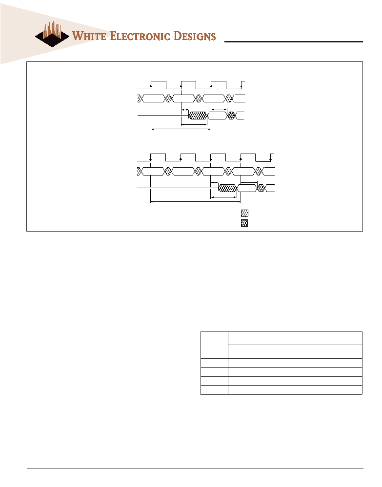
The CAS latency is the delay, in clock cycles, between the
registration of a READ command and the availability of the first
piece of output data. The latency can be set to two or three
clocks.
If a READ command is registered at clock edge
n, and the
latency is
m clocks, the data will be available by clock edge
n+m. The I/Os will start driving as a result of the clock edge
one cycle earlier (
n + m - 1), and provided that the relevant
access times are met, the data will be valid by clock edge
n
+ m. For example, assuming that the clock cycle time is such
that all relevant access times are met, if a READ command is
registered at T0 and the latency is programmed to two clocks,
the I/Os will start driving after T1 and the data will be valid by
T2. Table 2 below indicates the operating frequencies at
which each CAS latency setting can be used.
Reserved states should not be used as unknown operation or
incompatibility with future versions may result.
The normal operating mode is selected by setting M7and M8
to zero; the other combinations of values for M7 and M8 are
reserved for future use and/or test modes. The programmed
burst length applies to both READ and WRITE bursts.
Test modes and reserved states should not be used because
unknown operation or incompatibility with future versions
may result.
When M9 = 0, the burst length programmed via M0-M2
applies to both READ and WRITE bursts; when M9 = 1, the
programmed burst length applies to READ bursts, but write
accesses are single-location (nonburst) accesses.
The Truth Table provides a quick reference of available com-
mands. This is followed by a written description of each
command. Three additional Truth Tables appear following the
Operation section; these tables provide current state/next
state information.
FIG. 4 CAS LATENCY
CAS LATENCY
OPERATING MODE
WRITE BURST MODE
TABLE 2 - CAS LATENCY
ALLOWABLE OPERATING
FREQUENCY (MHZ)
CAS
SPEED
LATENCY = 2
LATENCY = 3
-66
≤ 50
≤ 66
-100
≤ 66
≤ 100
-125
≤ 100
≤ 125
-133
≤ 100
≤ 133
COMMANDS
CLK
Command
I/O
CLK
Command
I/O
T0
T1
T2
T3
T0
T1
T2
T3
T4
READ
NOP
CAS Latency = 2
DOUT
tLZ
tOH
tAC
READ
NOP
DOUT
tLZ
tOH
tAC
CAS Latency = 3
DON’T CARE
UNDEFINED
相关PDF资料 |
PDF描述 |
|---|---|
| W7NCF01GH11IS3CG | 64M X 16 FLASH 3.3V PROM CARD, 150 ns, UUC |
| W7NCF01GH11IS5DG | 64M X 16 FLASH 3.3V PROM CARD, 150 ns, UUC |
| W49F002UT12BN | 256K X 8 FLASH 5V PROM, 120 ns, PDSO32 |
| W3EG72255S202D3M | 256M X 72 DDR DRAM MODULE, 0.8 ns, DMA184 |
| W3EG72255S263D3M | 256M X 72 DDR DRAM MODULE, 0.75 ns, DMA184 |
相关代理商/技术参数 |
参数描述 |
|---|---|
| WEDPN16M72VR-66BI | 制造商:Microsemi Corporation 功能描述:16M X 72 SDRAM MODULE W/REGISTERED BUFFERS, 3.3V, 66 MHZ, 21 - Bulk |
| WEDPN16M72VR-66BM | 制造商:Microsemi Corporation 功能描述:16M X 72 SDRAM MODULE W/REGISTERED BUFFERS, 3.3V, 66 MHZ, 21 - Bulk |
| WEDPN16M72VR-XB2X | 制造商:WEDC 制造商全称:White Electronic Designs Corporation 功能描述:16MX72 REGISTERED SYNCHRONOUS DRAM |
| WEDPN16M72VR-XBX | 制造商:未知厂家 制造商全称:未知厂家 功能描述:Registered SDRAM MCP |
| WEDPN16M72V-XB2X | 制造商:WEDC 制造商全称:White Electronic Designs Corporation 功能描述:16Mx72 Synchronous DRAM |
发布紧急采购,3分钟左右您将得到回复。