- 您现在的位置:买卖IC网 > PDF目录276884 > WEDPN16M72VR-66BC (WHITE ELECTRONIC DESIGNS CORP) 16M X 72 SYNCHRONOUS DRAM MODULE, 7.5 ns, PBGA219 PDF资料下载
参数资料
| 型号: | WEDPN16M72VR-66BC |
| 厂商: | WHITE ELECTRONIC DESIGNS CORP |
| 元件分类: | DRAM |
| 英文描述: | 16M X 72 SYNCHRONOUS DRAM MODULE, 7.5 ns, PBGA219 |
| 封装: | 32 X 25 MM, PLASTIC, BGA-219 |
| 文件页数: | 9/13页 |
| 文件大小: | 161K |
| 代理商: | WEDPN16M72VR-66BC |
WEDPN16M72VR-XBX
White Electronic Designs Corporation (602) 437-1520 www.whiteedc.com
5
TABLE 1 - BURST DEFINITION
Burst
Starting Column
Order of Accesses Within a Burst
Length
Address
A0
2
0
0-1
1
1-0
A1
A0
0
0-1-2-3
4
0
1
1-2-3-0
1-0-3-2
1
0
2-3-0-1
1
3-0-1-2
3-2-1-0
A2
A1
A0
0
0-1-2-3-4-5-6-7
0
1
1-2-3-4-5-6-7-0
1-0-3-2-5-4-7-6
0
1
0
2-3-4-5-6-7-0-1
2-3-0-1-6-7-4-5
8
0
1
3-4-5-6-7-0-1-2
3-2-1-0-7-6-5-4
1
0
4-5-6-7-0-1-2-3
1
0
1
5-6-7-0-1-2-3-4
5-4-7-6-1-0-3-2
1
0
6-7-0-1-2-3-4-5
6-7-4-5-2-3-0-1
1
7-0-1-2-3-4-5-6
7-6-5-4-3-2-1-0
Full
n = A0-9/8/7
Cn, Cn + 1, Cn + 2
Page
Cn + 3, Cn + 4...
Not Supported
(y)
(location 0-y)
…Cn - 1,
Cn…
Type = Sequential
Type = Interleaved
M3 = 0
1
2
4
8
Reserved
Full Page
M3 = 1
1
2
4
8
Reserved
Operating Mode
Standard Operation
All other states reserved
0
-
0
-
Defined
-
0
1
Burst Type
Sequential
Interleaved
CAS Latency
Reserved
2
3
Reserved
Burst Length
M0
0
1
0
1
0
1
0
1
Burst Length
CAS Latency
BT
A9
A7
A6
A5
A4
A3
A8
A2
A1
A0
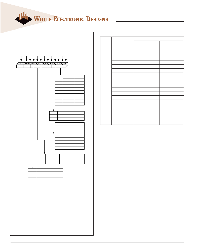
Mode Register (Mx)
Address Bus
M1
0
1
0
1
M2
0
1
M3
M4
0
1
0
1
0
1
0
1
M5
0
1
0
1
M6
0
1
M6-M0
M8
M7
Op Mode
A10
A11
Reserved* WB
0
1
Write Burst Mode
Programmed Burst Length
Single Location Access
M9
*Should program
M12, M11, M10 = 0, 0, 0
to ensure compatibility
with future devices.
Unused
WEDPN16M72MRD.eps
A12
FIG. 3 MODE REGISTER DEFINITION
NOTES:
1. For full-page accesses: y = 512.
2. For a burst length of two, A1-8 select the block-of-two burst; A0 selects the
starting column within the block.
3. For a burst length of four, A2-8 select the block-of-four burst; A0-1 select the
starting column within the block.
4. For a burst length of eight, A3-8 select the block-of-eight burst; A0-2 select
the starting column within the block.
5. For a full-page burst, the full row is selected and A0-8 select the starting
column.
6. Whenever a boundary of the block is reached within a given sequence
above, the following access wraps within the block.
7. For a burst length of one, A0-8 select the unique column to be accessed, and
Mode Register bit M3 is ignored.
相关PDF资料 |
PDF描述 |
|---|---|
| W7NCF01GH11IS3CG | 64M X 16 FLASH 3.3V PROM CARD, 150 ns, UUC |
| W7NCF01GH11IS5DG | 64M X 16 FLASH 3.3V PROM CARD, 150 ns, UUC |
| W49F002UT12BN | 256K X 8 FLASH 5V PROM, 120 ns, PDSO32 |
| W3EG72255S202D3M | 256M X 72 DDR DRAM MODULE, 0.8 ns, DMA184 |
| W3EG72255S263D3M | 256M X 72 DDR DRAM MODULE, 0.75 ns, DMA184 |
相关代理商/技术参数 |
参数描述 |
|---|---|
| WEDPN16M72VR-66BI | 制造商:Microsemi Corporation 功能描述:16M X 72 SDRAM MODULE W/REGISTERED BUFFERS, 3.3V, 66 MHZ, 21 - Bulk |
| WEDPN16M72VR-66BM | 制造商:Microsemi Corporation 功能描述:16M X 72 SDRAM MODULE W/REGISTERED BUFFERS, 3.3V, 66 MHZ, 21 - Bulk |
| WEDPN16M72VR-XB2X | 制造商:WEDC 制造商全称:White Electronic Designs Corporation 功能描述:16MX72 REGISTERED SYNCHRONOUS DRAM |
| WEDPN16M72VR-XBX | 制造商:未知厂家 制造商全称:未知厂家 功能描述:Registered SDRAM MCP |
| WEDPN16M72V-XB2X | 制造商:WEDC 制造商全称:White Electronic Designs Corporation 功能描述:16Mx72 Synchronous DRAM |
发布紧急采购,3分钟左右您将得到回复。