- 您现在的位置:买卖IC网 > PDF目录276884 > WEDPN16M72VR-66BC (WHITE ELECTRONIC DESIGNS CORP) 16M X 72 SYNCHRONOUS DRAM MODULE, 7.5 ns, PBGA219 PDF资料下载
参数资料
| 型号: | WEDPN16M72VR-66BC |
| 厂商: | WHITE ELECTRONIC DESIGNS CORP |
| 元件分类: | DRAM |
| 英文描述: | 16M X 72 SYNCHRONOUS DRAM MODULE, 7.5 ns, PBGA219 |
| 封装: | 32 X 25 MM, PLASTIC, BGA-219 |
| 文件页数: | 3/13页 |
| 文件大小: | 161K |
| 代理商: | WEDPN16M72VR-66BC |
WEDPN16M72VR-XBX
White Electronic Designs Corporation (602) 437-1520 www.whiteedc.com
11
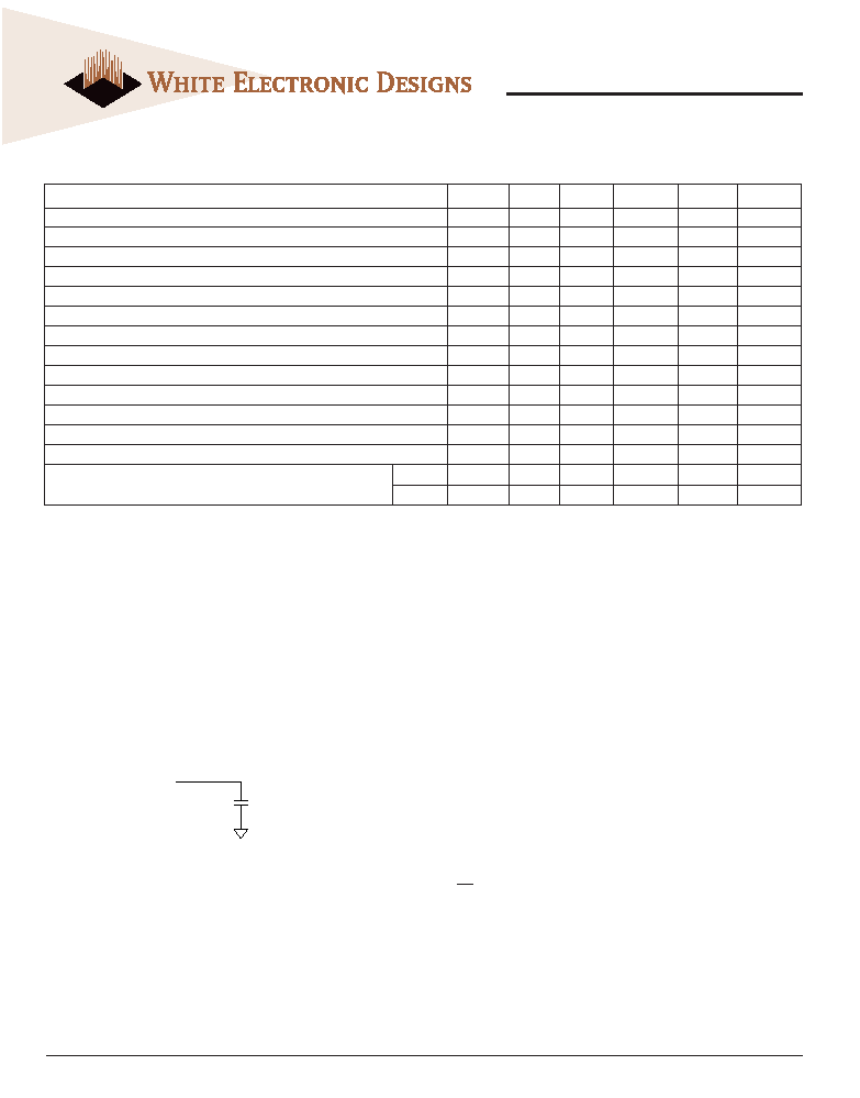
AC FUNCTIONAL CHARACTERISTICS (NOTES 5,6,7,8,9,11, 29)
Parameter/Condition
Symbol
-133
-125
-100
-66
Units
READ/WRITE command to READ/WRITE command (17)
tCCD
1
11tCK
CKE to clock disable or power-down entry mode (14)
tCKED
1
11tCK
CKE to clock enable or power-down exit setup mode (14)
tPED
1
11tCK
DQM to input data delay (17)
tDQD
0
00tCK
DQM to data mask during WRITEs
tDQM
0
00tCK
DQM to data high-impedance during READs
tDQZ
2
22tCK
WRITE command to input data delay (17)
tDWD
0
00tCK
Data-in to ACTIVE command (15)
tDAL
5
44tCK
Data-in to PRECHARGE command (16)
tDPL
2
22tCK
Last data-in to burst STOP command (17)
tBDL
1
11tCK
Last data-in to new READ/WRITE command (17)
tCDL
1
11tCK
Last data-in to PRECHARGE command (16)
tRDL
2
22tCK
LOAD MODE REGISTER command to ACTIVE or REFRESH command (25)
tMRD
2
22tCK
Data-out to high-impedance from PRECHARGE command (17)
CL = 3
tROH
33
3
tCK
CL = 2
tROH
22
2
-
tCK
NOTES:
1. All voltages referenced to VSS.
2. This parameter is not tested but guaranteed by design. f = 1 MHz, TA = 25°C.
3. IDD is dependent on output loading and cycle rates. Specified values are
obtained with minimum cycle time and the outputs open.
4. Enables on-chip refresh and address counters.
5. The minimum specifications are used only to indicate cycle time at which
proper operation over the full temperature range is ensured.
6. An initial pause of 100s is required after power-up, followed by two AUTO
REFRESH commands, before proper device operation is ensured. (VCC must be
powered up simultaneously.) The two AUTO REFRESH command wake-ups
should be repeated any time the tREF refresh requirement is exceeded.
7. AC characteristics assume tT = 1ns.
8. In addition to meeting the transition rate specification, the clock and CKE must
transit between VIH and VIL (or between VIL and VIH) in a monotonic manner.
9. Outputs measured at 1.5V with equivalent load:
10. tHZ defines the time at which the output achieves the open circuit
condition; it is not a reference to VOH or VOL. The last valid data element will
meet tOH before going High-Z.
11. AC timing and IDD tests have VIL = 0V and VIH = 3V, with timing referenced
to 1.5V crossover point.
12. Other input signals are allowed to transition no more than once every two
clocks and are otherwise at valid VIH or VIL levels.
13. ICC specifications are tested after the device is properly initialized.
14. Timing actually specified by tCKS; clock(s) specified as a reference only at
minimum cycle rate.
15. Timing actually specified by tWR plus tRP; clock(s) specified as a reference
only at minimum cycle rate.
16. Timing actually specified by tWR.
17. Required clocks are specified by JEDEC functionality and are not dependent
on any timing parameter.
18. The ICC current will decrease as the CAS latency is reduced. This is due to
the fact that the maximum cycle rate is slower as the CAS latency is reduced.
19. Address transitions average one transition every two clocks.
20. CLK must be toggled a minimum of two times during this period.
21. VIH overshoot: VIH (MAX) = VCC + 2V for a pulse width - 3ns, and the
pulse width cannot be greater than one third of the cycle rate. VIL undershoot:
VIL (MIN) = -2V for a pulse width - 3ns.
22. The clock frequency must remain constant (stable clock is defined as a
signal cycling within timing constraints specified for the clock pin) during access
or precharge states (READ, WRITE, including tWR, and PRECHARGE commands).
CKE may be used to reduce the data rate.
23. Auto precharge mode only. The precharge timing budget (tRP) begins 7.5ns/
7ns after the first clock delay, after the last WRITE is executed.
24. Precharge mode only.
25. JEDEC and PC100 specify three clocks.
26. Parameter guaranteed by design.
27. Self refresh available in commercial and industrial temperatures only.
28. OE high.
29. All AC timings do not count extra clock cycle needed on control signals to
be registered.
Q
50pF
相关PDF资料 |
PDF描述 |
|---|---|
| W7NCF01GH11IS3CG | 64M X 16 FLASH 3.3V PROM CARD, 150 ns, UUC |
| W7NCF01GH11IS5DG | 64M X 16 FLASH 3.3V PROM CARD, 150 ns, UUC |
| W49F002UT12BN | 256K X 8 FLASH 5V PROM, 120 ns, PDSO32 |
| W3EG72255S202D3M | 256M X 72 DDR DRAM MODULE, 0.8 ns, DMA184 |
| W3EG72255S263D3M | 256M X 72 DDR DRAM MODULE, 0.75 ns, DMA184 |
相关代理商/技术参数 |
参数描述 |
|---|---|
| WEDPN16M72VR-66BI | 制造商:Microsemi Corporation 功能描述:16M X 72 SDRAM MODULE W/REGISTERED BUFFERS, 3.3V, 66 MHZ, 21 - Bulk |
| WEDPN16M72VR-66BM | 制造商:Microsemi Corporation 功能描述:16M X 72 SDRAM MODULE W/REGISTERED BUFFERS, 3.3V, 66 MHZ, 21 - Bulk |
| WEDPN16M72VR-XB2X | 制造商:WEDC 制造商全称:White Electronic Designs Corporation 功能描述:16MX72 REGISTERED SYNCHRONOUS DRAM |
| WEDPN16M72VR-XBX | 制造商:未知厂家 制造商全称:未知厂家 功能描述:Registered SDRAM MCP |
| WEDPN16M72V-XB2X | 制造商:WEDC 制造商全称:White Electronic Designs Corporation 功能描述:16Mx72 Synchronous DRAM |
发布紧急采购,3分钟左右您将得到回复。