- 您现在的位置:买卖IC网 > PDF目录276877 > WEDPN4M72V-100B2M (WHITE ELECTRONIC DESIGNS CORP) 4M X 72 SYNCHRONOUS DRAM, 7 ns, PBGA219 PDF资料下载
参数资料
| 型号: | WEDPN4M72V-100B2M |
| 厂商: | WHITE ELECTRONIC DESIGNS CORP |
| 元件分类: | DRAM |
| 英文描述: | 4M X 72 SYNCHRONOUS DRAM, 7 ns, PBGA219 |
| 封装: | 21 X 21 MM, PLASTIC, BGA-219 |
| 文件页数: | 2/15页 |
| 文件大小: | 403K |
| 代理商: | WEDPN4M72V-100B2M |
10
White Electronic Designs Corporation (602) 437-1520 www.whiteedc.com
White Electronic Designs
WEDPN4M72V-XB2X
January 2005
Rev. 2
White Electronic Designs Corp. reserves the right to change products or specications without notice.
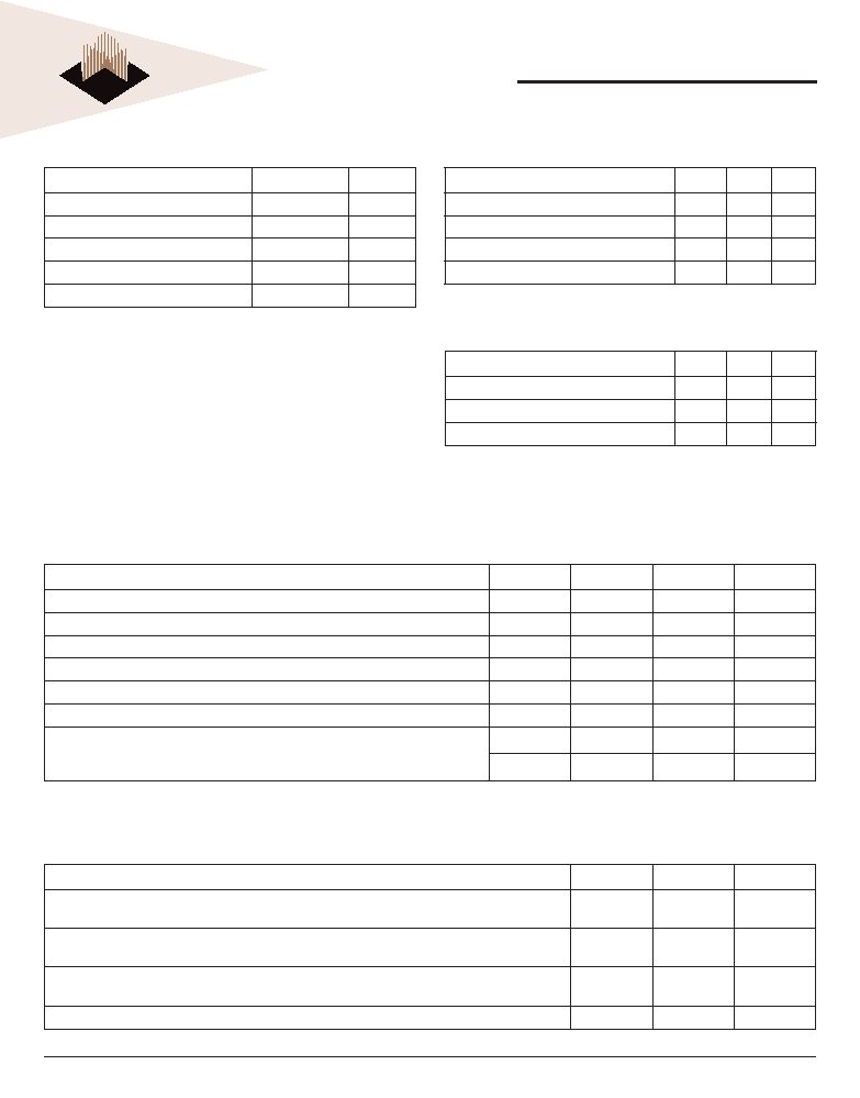
DC ELECTRICAL CHARACTERISTICS AND OPERATING CONDITIONS (NOTES 1, 6)
VCC = +3.3V ± 0.3V; -55°C ≤ TA ≤ +125°C
Parameter/Condition
Symbol
Min
Max
Units
Supply Voltage
VCC
3
3.6
V
Input High Voltage: Logic 1; All inputs (21)
VIH
2VCC + 0.3
V
Input Low Voltage: Logic 0; All inputs (21)
VIL
-0.3
0.8
V
Input Leakage Current: Any input 0V ≤ VIN ≤ VCC (All other pins not under test = 0V)
II
-5
5
μA
Input Leakage Address Current (All other pins not under test = 0V)
II
-25
25
μA
Output Leakage Current: I/Os are disabled; 0V ≤ VOUT ≤ VCCQ
IOZ
-5
5
μA
Output Levels:
Output High Voltage (IOUT = -4mA)
Output Low Voltage (IOUT = 4mA)
VOH
2.4
–
V
VOL
–
0.4
V
ICC SPECIFICATIONS AND CONDITIONS (NOTES 1, 6, 11, 13)
VCC = +3.3V ± 0.3V; -55°C ≤ TA ≤ +125°C
Parameter/Condition
Symbol
Max
Units
Operating Current: Active Mode;
Burst = 2; Read or Write; tRC = tRC (min); CAS latency = 3 (3, 18, 19)
ICC1
575
mA
Standby Current: Active Mode; CKE = HIGH; CS# = HIGH;
All banks active after tRCD met; No accesses in progress (3, 12, 19)
ICC3
225
mA
Operating Current: Burst Mode; Continuous burst;
Read or Write; All banks active; CAS latency = 3 (3, 18, 19)
ICC4
700
mA
Self Refresh Current: CKE 0.2V Commercial and Industrial temperature only (27)
ICC7
5mA
ABSOLUTE MAXIMUM RATINGS
Parameter
Unit
Voltage on VCC Supply relative to VSS
-1 to 4.6
V
Voltage on NC or I/O pins relative to VSS
-1 to 4.6
V
Operating Temperature TA (Mil)
-55 to +125
°C
Operating Temperature TA (Ind)
-40 to +85
°C
Storage Temperature, Plastic
-55 to +125
°C
NOTE:
Stress greater than those listed under "Absolute Maximum Ratings" may cause
permanent damage to the device. This is a stress rating only and functional operation
of the device at these or any other conditions greater than those indicated in the
operational sections of this specication is not implied. Exposure to absolute maximum
rating conditions for extended periods may affect reliability.
CAPACITANCE (NOTE 2)
Parameter
Symbol
Max
Unit
Input Capacitance: CK
CI1
6
pF
Addresses, BA0-1 Input Capacitance
CA
20
pF
Input Capacitance: All other input-only pins
CI2
7
pF
Input/Output Capacitance: I/Os
CIO
8
pF
THERMAL RESISTANCE
Description
Symbol
Max
Unit
Thermal Resistance: Die Junction to Ambient
θJA
17.5
°C/W
Thermal Resistance: Die Junction to Ball
θJB
12.3
°C/W
Thermal Resistance: Die Junction to Case
θJC
8.6
°C/W
NOTE: Refer to Application Note “PBGA Thermal Resistance Corrleation” for further
information regarding WEDC’s thermal modeling.
相关PDF资料 |
PDF描述 |
|---|---|
| WE32K32N-120G2UQ | EEPROM 5V MODULE, CQFP68 |
| W3EG264M72AFSR262D3SG | 128M X 72 DDR DRAM MODULE, 0.75 ns, DMA184 |
| W3EG264M72AFSR265D3SG | 128M X 72 DDR DRAM MODULE, 0.75 ns, DMA184 |
| WED3EG72M18S265JD3SG | 16M X 72 DDR DRAM MODULE, 0.75 ns, DMA184 |
| WS512K32-17G2I | 2M X 8 MULTI DEVICE SRAM MODULE, 17 ns, CQFP68 |
相关代理商/技术参数 |
参数描述 |
|---|---|
| WEDPN4M72V-125B2C | 制造商:WEDC 制造商全称:White Electronic Designs Corporation 功能描述:4Mx72 Synchronous DRAM |
| WEDPN4M72V-125B2I | 制造商:Microsemi Corporation 功能描述:4M X 72 SDRAM MODULE, 3.3V, 121 MHZ, 219 PBGA 21MM X 21MM, I - Bulk |
| WEDPN4M72V-125B2M | 制造商:Microsemi Corporation 功能描述:4M X 72 SDRAM MODULE, 3.3V, 121 MHZ, 219 PBGA 21MM X 21MM, M - Bulk |
| WEDPN4M72V-133B2C | 制造商:WEDC 制造商全称:White Electronic Designs Corporation 功能描述:4Mx72 Synchronous DRAM |
| WEDPN4M72V-133B2I | 制造商:WEDC 制造商全称:White Electronic Designs Corporation 功能描述:4Mx72 Synchronous DRAM |
发布紧急采购,3分钟左右您将得到回复。