参数资料
| 型号: | X40035S14I-BT1 |
| 厂商: | Intersil |
| 文件页数: | 11/23页 |
| 文件大小: | 0K |
| 描述: | IC VOLTAGE MONITOR TRPL 14-SOIC |
| 标准包装: | 2,500 |
| 类型: | 多压监控器 |
| 监视电压数目: | 3 |
| 输出: | 开路漏极或开路集电极 |
| 复位: | 低有效 |
| 复位超时: | 可调节/可选择 |
| 电压 - 阀值: | 1.3V,2.9V,4.6V |
| 工作温度: | -40°C ~ 85°C |
| 安装类型: | 表面贴装 |
| 封装/外壳: | 14-SOIC(0.154",3.90mm 宽) |
| 供应商设备封装: | 14-SOICN |
| 包装: | 带卷 (TR) |
�� �
�
�X40030,� X40031,� X40034,� X40035�
�WEL:� Write� Enable� Latch� (Volatile)�
�The� WEL� bit� controls� the� access� to� the� memory� and� to� the�
�Register� during� a� write� operation.� This� bit� is� a� volatile� latch�
�that� powers� up� in� the� LOW� (disabled)� state.� While� the� WEL�
�bit� is� LOW,� writes� to� any� address,� including� any� control�
�registers� will� be� ignored� (no� acknowledge� will� be� issued� after�
�the� Data� Byte).� The� WEL� bit� is� set� by� writing� a� “1”� to� the�
�WEL� bit� and� zeroes� to� the� other� bits� of� the� control� register.�
�Once� set,� WEL� remains� set� until� either� it� is� reset� to� 0� (by�
�writing� a� “0”� to� the� WEL� bit� and� zeroes� to� the� other� bits� of� the�
�control� register)� or� until� the� part� powers� up� again.� Writes� to�
�the� WEL� bit� do� not� cause� a� high� voltage� write� cycle,� so� the�
�device� is� ready� for� the� next� operation� immediately� after� the�
�stop� condition.�
�PUP1,� PUP0:� Power-Up� Bits� (Nonvolatile)�
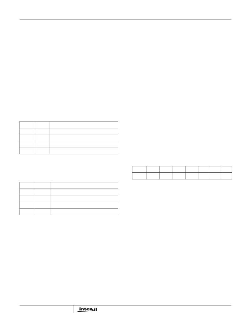
�The� Power-up� bits,� PUP1� and� PUP0,� determine� the� t� PURST�
�time� delay.� The� nominal� power-up� times� are� shown� in� Table� 2.�
�TABLE� 2.� NOMINAL� POWER-UP� TIMES�
�bits.� This� operation� proceeded� by� a� start� and� ended� with� a�
�stop� bit.� Since� this� is� a� nonvolatile� write� cycle� it� will� take� up�
�to� 10ms� (max.)� to� complete.� The� RWEL� bit� is� reset� by� this�
�cycle� and� the� sequence� must� be� repeated� to� change� the�
�nonvolatile� bits� again.� If� bit� 2� is� set� to� ‘1’� in� this� third� step�
�(� qxys� 0� 11� r� )� then� the� RWEL� bit� is� set,� but� the� WD1,� WD0,�
�PUP1,� PUP0,� and� BP� bits� remain� unchanged.� Writing� a�
�second� byte� to� the� control� register� is� not� allowed.� Doing� so�
�aborts� the� write� operation� and� returns� a� NACK.�
�?� A� read� operation� occurring� between� any� of� the� previous�
�operations� will� not� interrupt� the� register� write� operation.�
�?� The� RWEL� bit� cannot� be� reset� without� writing� to� the�
�nonvolatile� control� bits� in� the� control� register,� or� power�
�cycling� the� device� or� attempting� a� write� to� a� write�
�protected� block.�
�To� illustrate,� a� sequence� of� writes� to� the� device� consisting� of�
�[02H,� 06H,� 02H]� will� reset� all� of� the� nonvolatile� bits� in� the�
�Control� Register� to� 0.� A� sequence� of� [02H,� 06H,� 06H]� will�
�leave� the� nonvolatile� bits� unchanged� and� the� RWEL� bit�
�remains� set.�
�PUP1�
�0�
�0�
�1�
�1�
�PUP0�
�0�
�1�
�0�
�1�
�POWER-ON� RESET� DELAY� (� t� PURST� )�
�50ms�
�200ms� (factory� setting)�
�400ms�
�800ms�
�Note:� t� PURST� is� set� to� 200ms� as� factory� default.� Watchdog�
�Timer� bits� are� shipped� disabled.�
�Fault� Detection� Register� (FDR)�
�The� Fault� Detection� Register� provides� the� user� the� status� of�
�what� causes� the� system� reset� active.� The� Manual� Reset�
�Fail,� Watchdog� Timer� Fail� and� Three� Low� Voltage� Fail� bits�
�WD1,� WD0:� Watchdog� Timer� Bits� (Nonvolatile)�
�are� volatile.�
�The� bits� WD1� and� WD0� control� the� period� of� the� Watchdog�
�Timer.� The� options� are� shown� in� Table� 3.�
�TABLE� 3.� WATCHDOG� TIMER� OPTIONS�
�7�
�LV1F�
�6�
�LV2F�
�5�
�LV3F�
�4�
�WDF�
�3�
�MRF�
�2�
�0�
�1�
�0�
�0�
�0�
�WD1�
�0�
�0�
�1�
�1�
�WD0�
�0�
�1�
�0�
�1�
�WATCHDOG� TIME� OUT� PERIOD�
�1.4s�
�200ms�
�25ms�
�Disabled� (factory� setting)�
�The� FDR� is� accessed� with� a� special� preamble� in� the� slave�
�byte� (1011)� and� is� located� at� address� 0FFh.� It� can� only� be�
�modified� by� performing� a� byte� write� operation� directly� to� the�
�address� of� the� register� and� only� one� data� byte� is� allowed� for�
�each� register� write� operation.�
�There� is� no� need� to� set� the� WEL� or� RWEL� in� the� control�
�register� to� access� this� FDR.�
�Writing� to� the� Control� Registers�
�Changing� any� of� the� nonvolatile� bits� of� the� control� and� trickle�
�registers� requires� the� following� steps:�
�?� Write� a� 02H� to� the� Control� Register� to� set� the� Write� Enable�
�Latch� (WEL).� This� is� a� volatile� operation,� so� there� is� no�
�delay� after� the� write� (operation� preceded� by� a� start� and�
�ended� with� a� stop).�
�?� Write� a� 06H� to� the� Control� Register� to� set� the� Register�
�Write� Enable� Latch� (RWEL)� and� the� WEL� bit.� This� is� also�
�a� volatile� cycle.� The� zeros� in� the� data� byte� are� required�
�(operation� proceeded� by� a� start� and� ended� with� a� stop).�
�?� Write� one� byte� value� to� the� Control� Register� that� has� all�
�the� control� bits� set� to� the� desired� state.� The� Control�
�register� can� be� represented� as� qxys� 001� r� in� binary,� where�
�xy� are� the� WD� bits,� s� is� the� BP� bit� and� qr� are� the� power-up�
�11�
�At� power-up,� the� FDR� is� defaulted� to� all� “0”.� The� system�
�needs� to� initialize� this� register� to� all� “1”� before� the� actual�
�monitoring� can� take� place.� In� the� event� of� any� one� of� the�
�monitored� sources� fail,� the� corresponding� bit� in� the� register�
�will� change� from� a� “1”� to� a� “0”� to� indicate� the� failure.� At� this�
�moment,� the� system� should� perform� a� read� to� the� register�
�and� note� the� cause� of� the� reset.� After� reading� the� register,�
�the� system� should� reset� the� register� back� to� all� “1”� again.�
�The� state� of� the� FDR� can� be� read� at� any� time� by� performing�
�a� random� read� at� address� 0FFh,� using� the� special� preamble.�
�The� FDR� can� be� read� by� performing� a� random� read� at� 0FFh�
�address� of� the� register� at� any� time.� Only� one� byte� of� data� is�
�read� by� the� register� read� operation.�
�FN8114.2�
�August� 25,� 2008�
�相关PDF资料 |
PDF描述 |
|---|---|
| EBA36DTAD-S273 | CONN EDGECARD 72POS R/A .125 SLD |
| X40035S14I-B | IC VOLTAGE MONITOR TRPL 14-SOIC |
| X40034V14I-CT1 | IC VOLTAGE MONITOR TRPL 14-TSSOP |
| ISL6363IRTZ | IC CONTROLLER VR12 48TQFN |
| RBM44DSES-S243 | CONN EDGECARD 88POS .156 EYELET |
相关代理商/技术参数 |
参数描述 |
|---|---|
| X40035S14I-C | 功能描述:IC VOLTAGE MONITOR TRPL 14-SOIC RoHS:否 类别:集成电路 (IC) >> PMIC - 监控器 系列:- 标准包装:100 系列:- 类型:简单复位/加电复位 监视电压数目:1 输出:- 复位:低有效 复位超时:最小为 100 ms 电压 - 阀值:4.38V 工作温度:0°C ~ 70°C 安装类型:表面贴装 封装/外壳:8-TSSOP(0.173",4.40mm 宽) 供应商设备封装:8-TSSOP 包装:管件 |
| X40035S14I-CT1 | 功能描述:IC VOLTAGE MONITOR TRPL 14-SOIC RoHS:否 类别:集成电路 (IC) >> PMIC - 监控器 系列:- 标准包装:100 系列:- 类型:简单复位/加电复位 监视电压数目:1 输出:- 复位:低有效 复位超时:最小为 100 ms 电压 - 阀值:4.38V 工作温度:0°C ~ 70°C 安装类型:表面贴装 封装/外壳:8-TSSOP(0.173",4.40mm 宽) 供应商设备封装:8-TSSOP 包装:管件 |
| X40035SA | 制造商:INTERSIL 制造商全称:Intersil Corporation 功能描述:Triple Voltage Monitor with Integrated CPU Supervisor |
| X40035SB | 制造商:INTERSIL 制造商全称:Intersil Corporation 功能描述:Triple Voltage Monitor with Integrated CPU Supervisor |
| X40035SC | 制造商:INTERSIL 制造商全称:Intersil Corporation 功能描述:Triple Voltage Monitor with Integrated CPU Supervisor |
发布紧急采购,3分钟左右您将得到回复。