参数资料
| 型号: | X4005S8I-4.5A |
| 厂商: | Intersil |
| 文件页数: | 9/16页 |
| 文件大小: | 0K |
| 描述: | IC SUPERVISOR CPU I2C 8-SOIC |
| 标准包装: | 100 |
| 类型: | 简单复位/加电复位 |
| 监视电压数目: | 1 |
| 输出: | 开路漏极或开路集电极 |
| 复位: | 高有效 |
| 复位超时: | 最小为 100 ms |
| 电压 - 阀值: | 4.62V |
| 工作温度: | -40°C ~ 85°C |
| 安装类型: | 表面贴装 |
| 封装/外壳: | 8-SOIC(0.154",3.90mm 宽) |
| 供应商设备封装: | 8-SOIC |
| 包装: | 管件 |
�� �
�
�X4003,� X4005�
�performed.� When� the� R/W� bit� is� a� one,� then� a� read�
�operation� is� selected.� A� zero� selects� a� write� operation.�
��?� After� loading� the� entire� slave� address� byte� from� the� SDA�
�bus,� the� device� compares� the� input� slave� byte� data� to� the�
�proper� slave� byte.� Upon� a� correct� compare,� the� device�
�outputs� an� acknowledge� on� the� SDA� line.�
�Write� Control� Register�
�To� write� to� the� control� register,� the� device� requires� the� slave�
�address� byte� and� a� byte� address.� This� gives� the� master�
�access� to� register.� After� receipt� of� the� address� byte,� the�
�device� responds� with� an� acknowledge,� and� awaits� the� data.�
�After� receiving� the� 8� bits� of� the� data� byte,� the� device� again�
�responds� with� an� acknowledge.� The� master� then� terminates�
�the� transfer� by� generating� a� stop� condition,� at� which� time� the�
�device� begins� the� internal� write� cycle� to� the� nonvolatile� memory.�
�During� this� internal� write� cycle,� the� device� inputs� are� disabled,�
�so� the� device� will� not� respond� to� any� requests� from� the� master.�
�If� WP� is� HIGH,� the� control� register� cannot� be� changed.� A� write�
�to� the� control� register� will� suppress� the� acknowledge� bit� and� no�
�data� in� the� control� register� will� change.� With� WP� low,� a� second�
�byte� written� to� the� control� register� terminates� the� operation� and�
�no� write� occurs.�
�Stops� and� Write� Modes�
�Stop� conditions� that� terminate� write� operations� must� be� sent� by�
�the� master� after� sending� 1� full� data� byte� plus� the� subsequent�
�ACK� signal.� If� a� stop� is� issued� in� the� middle� of� a� data� byte,� or�
�before� 1� full� data� byte� plus� its� associated� ACK� is� sent,� then� the�
�device� will� reset� itself� without� performing� the� write.�
�condition.� Refer� to� Figure� 10� for� the� address,� acknowledge,�
�and� data� transfer� sequences.�
�Operational� Notes�
�The� device� powers-up� in� the� following� state:�
�?� The� device� is� in� the� low� power� standby� state.�
�?� The� WEL� bit� is� set� to� ‘0’.� In� this� state� it� is� not� possible� to�
�write� to� the� device.�
�?� SDA� pin� is� the� input� mode.�
�RESET/RESET� signal� is� active� for� t� PURST� .�
�Data� Protection�
�The� following� circuitry� has� been� included� to� prevent�
�inadvertent� writes:�
�?� The� WEL� bit� must� be� set� to� allow� a� write� operation.�
�?� The� proper� clock� count� and� bit� sequence� is� required� prior�
�to� the� stop� bit� in� order� to� start� a� nonvolatile� write� cycle.�
�?� A� three� step� sequence� is� required� before� writing� into� the�
�control� register� to� change� watchdog� timer� or� block� lock�
�settings.�
�?� The� WP� pin,� when� held� HIGH,� prevents� all� writes� to� the�
�control� register.�
�?� Communication� to� the� device� is� inhibited� below� the� V� TRIP�
�voltage.�
�?� Command� to� change� the� control� register� are� terminated� if�
�in-progress� when� RESET/RESET� go� active.�
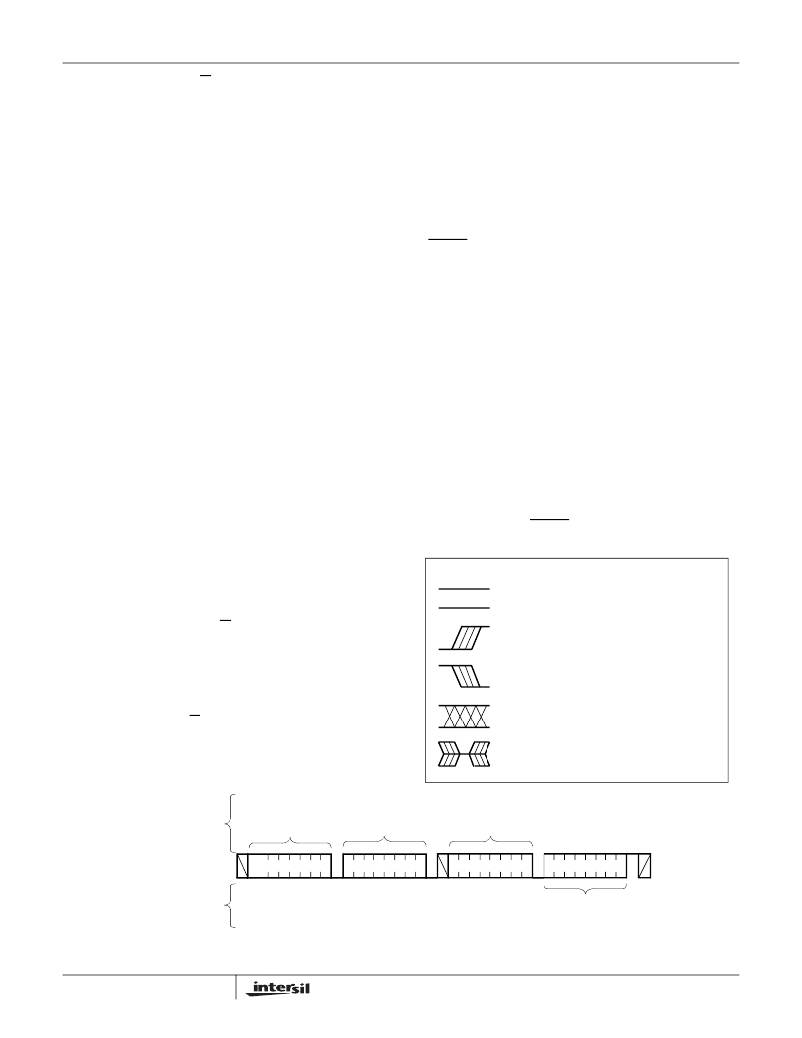
�Symbol� Table�
�Serial� Read� Operations�
�The� read� operation� allows� the� master� to� access� the� control�
�register.� To� conform� to� the� I� 2� C� standard,� prior� to� issuing� the�
�slave� address� byte� with� the� R/W� bit� set� to� one,� the� master�
�must� first� perform� a� “dummy”� write� operation.� The� master�
�issues� the� start� condition� and� the� slave� address� byte,�
�receives� an� acknowledge,� then� issues� the� byte� address.�
�After� acknowledging� receipt� of� the� byte� address,� the� master�
�immediately� issues� another� start� condition� and� the� slave�
�address� byte� with� the� R/W� bit� set� to� one.� This� is� followed� by�
�an� acknowledge� from� the� device� and� then� by� the� eight� bit�
�control� register.� The� master� terminates� the� read� operation� by�
�not� responding� with� an� acknowledge� and� then� issuing� a� stop�
�WAVEFORM�
�INPUTS�
�Must� be�
�steady�
�May� change�
�from� LOW�
�to� HIGH�
�May� change�
�from� HIGH�
�to� LOW�
�Don’t� Care:�
�Changes�
�Allowed�
�N/A�
�OUTPUTS�
�Will� be�
�steady�
�Will� change�
�from� LOW�
�to� HIGH�
�Will� change�
�from� HIGH�
�to� LOW�
�Changing:�
�State� Not�
�Known�
�Center� Line�
�is� High�
�Impedance�
�SIGNALS�
�FROM� THE�
�MASTER�
�S�
�T�
�A�
�R�
�T�
�SLAVE�
�ADDRESS�
�BYTE�
�ADDRESS�
�S�
�T�
�A�
�R�
�T�
�SLAVE�
�ADDRESS�
�S�
�T�
�O�
�P�
�SDA� BUS�
�1� 0� 1� 1� 0� 0� 1� 0�
�1� 1� 1� 1� 1� 1� 1� 1�
�1� 0� 1� 1� 0� 0� 1� 1�
�SIGNALS�
�FROM� THE�
�A�
�C�
�K�
�A�
�C�
�K�
�A�
�C�
�K�
�DATA�
�SLAVE�
�FIGURE� 10.� CONTROL� REGISTER� READ� SEQUENCE�
�9�
�FN8113.2�
�June� 30,� 2008�
�相关PDF资料 |
PDF描述 |
|---|---|
| X40239S16I-BT1 | IC VOLTAGE MON TRPL EE 16-SOIC |
| X40415V8I-CT1 | IC VOLTAGE MON DUAL W/SUP 8TSSOP |
| X40421V14I-CT1 | IC VOLT MON DUAL SUP/SW 14-TSSOP |
| X40435V14I-CT1 | IC VOLT MON TRPL EEPROM 14-TSSOP |
| X4045S8T1 | IC SUPERVISOR CPU 4K EE 8-SOIC |
相关代理商/技术参数 |
参数描述 |
|---|---|
| X4005S8IZ | 功能描述:IC SUPERVISOR CPU I2C 8-SOIC RoHS:是 类别:集成电路 (IC) >> PMIC - 监控器 系列:- 产品培训模块:Lead (SnPb) Finish for COTS Obsolescence Mitigation Program 标准包装:2,500 系列:- 类型:简单复位/加电复位 监视电压数目:1 输出:开路漏极或开路集电极 复位:低有效 复位超时:最小为 600 ms 电压 - 阀值:3.8V 工作温度:-40°C ~ 85°C 安装类型:表面贴装 封装/外壳:SC-74A,SOT-753 供应商设备封装:SOT-23-5 包装:带卷 (TR) |
| X4005S8IZ-2.7 | 功能描述:IC SUPERVISOR CPU I2C 8-SOIC RoHS:是 类别:集成电路 (IC) >> PMIC - 监控器 系列:- 产品培训模块:Lead (SnPb) Finish for COTS Obsolescence Mitigation Program 标准包装:2,500 系列:- 类型:简单复位/加电复位 监视电压数目:1 输出:开路漏极或开路集电极 复位:低有效 复位超时:最小为 600 ms 电压 - 阀值:3.8V 工作温度:-40°C ~ 85°C 安装类型:表面贴装 封装/外壳:SC-74A,SOT-753 供应商设备封装:SOT-23-5 包装:带卷 (TR) |
| X4005S8IZ-2.7A | 功能描述:IC SUPERVISOR CPU I2C 8-SOIC RoHS:是 类别:集成电路 (IC) >> PMIC - 监控器 系列:- 产品培训模块:Lead (SnPb) Finish for COTS Obsolescence Mitigation Program 标准包装:2,500 系列:- 类型:简单复位/加电复位 监视电压数目:1 输出:开路漏极或开路集电极 复位:低有效 复位超时:最小为 600 ms 电压 - 阀值:3.8V 工作温度:-40°C ~ 85°C 安装类型:表面贴装 封装/外壳:SC-74A,SOT-753 供应商设备封装:SOT-23-5 包装:带卷 (TR) |
| X4005S8IZ-4.5A | 功能描述:IC SUPERVISOR CPU I2C 8-SOIC RoHS:是 类别:集成电路 (IC) >> PMIC - 监控器 系列:- 产品培训模块:Lead (SnPb) Finish for COTS Obsolescence Mitigation Program 标准包装:2,500 系列:- 类型:简单复位/加电复位 监视电压数目:1 输出:开路漏极或开路集电极 复位:低有效 复位超时:最小为 600 ms 电压 - 阀值:3.8V 工作温度:-40°C ~ 85°C 安装类型:表面贴装 封装/外壳:SC-74A,SOT-753 供应商设备封装:SOT-23-5 包装:带卷 (TR) |
| X4005S8Z | 功能描述:IC SUPERVISOR CPU I2C 8-SOIC RoHS:是 类别:集成电路 (IC) >> PMIC - 监控器 系列:- 产品培训模块:Lead (SnPb) Finish for COTS Obsolescence Mitigation Program 标准包装:2,500 系列:- 类型:简单复位/加电复位 监视电压数目:1 输出:开路漏极或开路集电极 复位:低有效 复位超时:最小为 600 ms 电压 - 阀值:3.8V 工作温度:-40°C ~ 85°C 安装类型:表面贴装 封装/外壳:SC-74A,SOT-753 供应商设备封装:SOT-23-5 包装:带卷 (TR) |
发布紧急采购,3分钟左右您将得到回复。