- 您现在的位置:买卖IC网 > PDF目录20009 > X9520V20I-B (Intersil)IC 3 DCP 2K EE LASR CTRL 20TSSOP PDF资料下载
参数资料
| 型号: | X9520V20I-B |
| 厂商: | Intersil |
| 文件页数: | 10/29页 |
| 文件大小: | 0K |
| 描述: | IC 3 DCP 2K EE LASR CTRL 20TSSOP |
| 标准包装: | 75 |
| 类型: | 激光二极管控制器(光纤) |
| 通道数: | 3 |
| 电源电压: | 2.7 V ~ 5.5 V |
| 电流 - 电源: | 1.5mA |
| 工作温度: | -40°C ~ 85°C |
| 封装/外壳: | 20-TSSOP(0.173",4.40mm 宽) |
| 供应商设备封装: | 20-TSSOP |
| 包装: | 管件 |
| 安装类型: | 表面贴装 |
第1页第2页第3页第4页第5页第6页第7页第8页第9页当前第10页第11页第12页第13页第14页第15页第16页第17页第18页第19页第20页第21页第22页第23页第24页第25页第26页第27页第28页第29页
�� �
�
�X9520�
�S�
�Signals� from� the�
�Master�
�t�
�a�
�r�
�t�
�Slave�
�Address�
�Address�
�Byte�
�Data�
�(1)�
�(2� <� n� <� 16)�
�Data�
�(n)�
�S�
�t�
�o�
�p�
�SDA� Bus�
�1� 0� 1� 0� 0� 0� 0� 0�
�Signals� from� the�
�Slave�
�A�
�C�
�K�
�A�
�C�
�K�
�A�
�C�
�K�
�A�
�C�
�K�
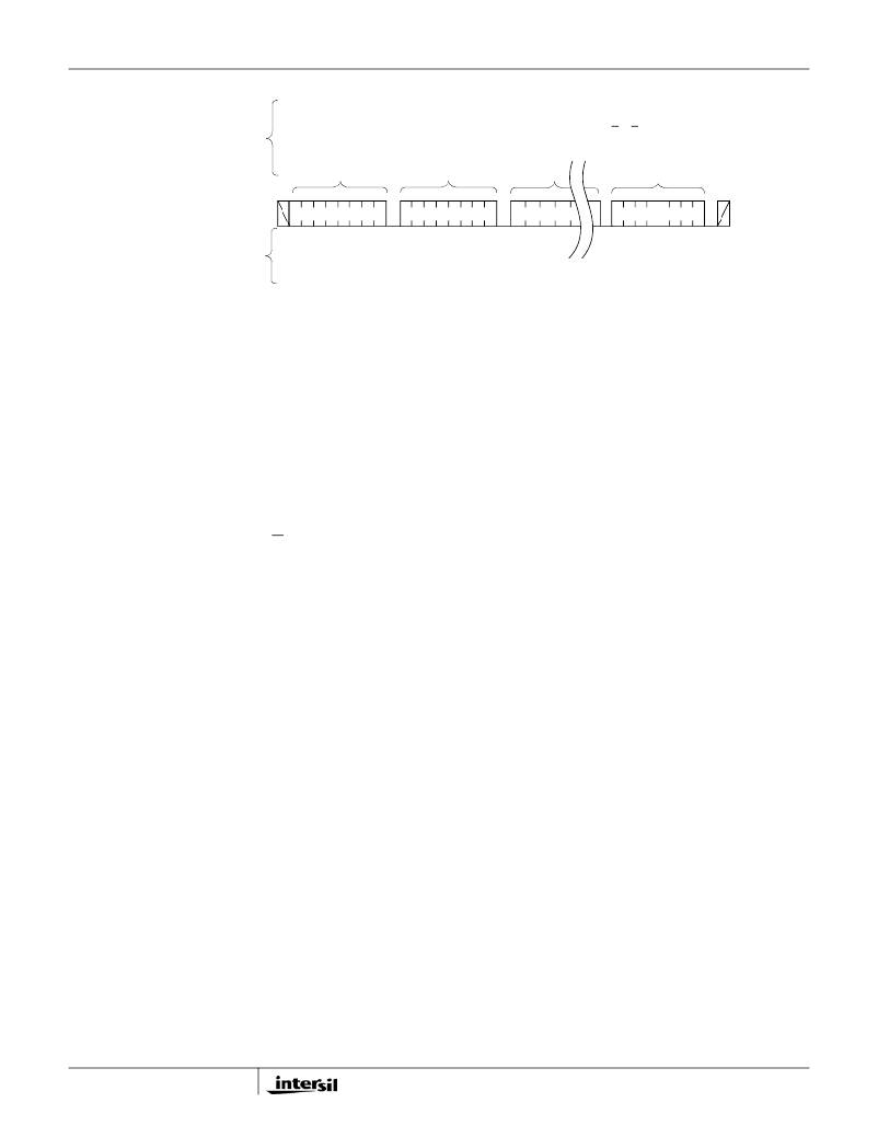
�FIGURE� 12.� EEPROM� PAGE� WRITE� OPERATION�
�It� should� be� noted� that� when� reading� out� the� data� byte� for�
�DCP0� (64� Tap),� the� upper� two� most� significant� bits� are�
�“unknown”� bits.� For� DCP1� (100� Tap),� the� upper� most�
�significant� bit� is� an� “unknown”.� For� DCP2� (256� Tap)� however,�
�all� bits� of� the� data� byte� are� relevant� (See� Figure� 10).�
�2KBIT� EEPROM� ARRAY�
�Operations� on� the� 2kbit� EEPROM� Array,� consist� of� either� 1,�
�2� or� 3� byte� command� sequences.� All� operations� on� the�
�EEPROM� must� begin� with� the� Device� Type� Identifier� of� the�
�Slave� Address� set� to� 1010000.� A� Read� or� Write� to� the�
�EEPROM� is� selected� by� setting� the� LSB� of� the� Slave�
�Address� to� the� appropriate� value� R/W� (Read� =� “1”,�
�Write� =� ”0”).�
�In� some� cases� when� performing� a� Read� or� Write� to� the�
�EEPROM,� an� Address� Byte� may� also� need� to� be� specified.�
�This� Address� Byte� can� contain� the� values� 00h� to� FFh.�
�EEPROM� BYTE� WRITE�
�In� order� to� perform� an� EEPROM� Byte� Write� operation� to� the�
�EEPROM� array,� the� Write� Enable� Latch� (WEL)� bit� of� the�
�CONSTAT� Register� must� first� be� set� (See� “BL1,� BL0:� Block�
�EEPROM� Page� Write�
�In� order� to� perform� an� EEPROM� Page� Write� operation� to� the�
�EEPROM� array,� the� Write� Enable� Latch� (WEL)� bit� of� the�
�CONSTAT� Register� must� first� be� set� (See� “BL1,� BL0:� Block�
�Lock� protection� bits� -� (Nonvolatile)”� on� page� 13.)�
�The� X9520� is� capable� of� a� page� write� operation.� It� is� initiated�
�in� the� same� manner� as� the� byte� write� operation;� but� instead�
�of� terminating� the� write� cycle� after� the� first� data� byte� is�
�transferred,� the� master� can� transmit� an� unlimited� number� of�
�8-bit� bytes.� After� the� receipt� of� each� byte,� the� X9520�
�responds� with� an� ACKNOWLEDGE,� and� the� address� is�
�internally� incremented� by� one.� The� page� address� remains�
�constant.� When� the� counter� reaches� the� end� of� the� page,� it�
�“rolls� over”� and� goes� back� to� ‘0’� on� the� same� page.�
�For� example,� if� the� master� writes� 12� bytes� to� the� page�
�starting� at� location� 11� (decimal),� the� first� 5� bytes� are� written�
�to� locations� 11� through� 15,� while� the� last� 7� bytes� are� written�
�to� locations� 0� through� 6.� Afterwards,� the� address� counter�
�would� point� to� location� 7.� If� the� master� supplies� more� than� 16�
�bytes� of� data,� then� new� data� overwrites� the� previous� data,�
�one� byte� at� a� time� (See� Figure� 13).�
�Lock� protection� bits� -� (Nonvolatile)”� on� page� 13.)�
�The� master� terminates� the� Data� Byte� loading� by� issuing� a�
�For� a� write� operation,� the� X9520� requires� the� Slave� Address�
�Byte� and� an� Address� Byte.� This� gives� the� master� access� to�
�any� one� of� the� words� in� the� array.� After� receipt� of� the�
�Address� Byte,� the� X9520� responds� with� an�
�ACKNOWLEDGE,� and� awaits� the� next� eight� bits� of� data.�
�After� receiving� the� 8� bits� of� the� Data� Byte,� it� again� responds�
�with� an� ACKNOWLEDGE.� The� master� then� terminates� the�
�transfer� by� generating� a� STOP� condition,� at� which� time� the�
�X9520� begins� the� internal� write� cycle� to� the� nonvolatile�
�memory� (See� Figure� 11).� During� this� internal� write� cycle,� the�
�X9520� inputs� are� disabled,� so� it� does� not� respond� to� any�
�requests� from� the� master.� The� SDA� output� is� at� high�
�impedance.� A� write� to� a� region� of� EEPROM� memory� which�
�has� been� protected� with� the� Block-Lock� feature� (See� “BL1,�
�BL0:� Block� Lock� protection� bits� -� (Nonvolatile)”� on� page� 13.),�
�suppresses� the� ACKNOWLEDGE� bit� after� the� Address� Byte.�
�10�
�STOP� condition,� which� causes� the� X9520� to� begin� the�
�nonvolatile� write� cycle.� As� with� the� byte� write� operation,� all�
�inputs� are� disabled� until� completion� of� the� internal� write�
�cycle.� See� Figure� 12� for� the� address,� ACKNOWLEDGE,� and�
�data� transfer� sequence.�
�Stops� and� EEPROM� Write� Modes�
�Stop� conditions� that� terminate� write� operations� must� be� sent�
�by� the� master� after� sending� at� least� 1� full� data� byte� and�
�receiving� the� subsequent� ACKNOWLEDGE� signal.� If� the�
�master� issues� a� STOP� within� a� Data� Byte,� or� before� the�
�X9520� issues� a� corresponding� ACKNOWLEDGE,� the� X9520�
�cancels� the� write� operation.� Therefore,� the� contents� of� the�
�EEPROM� array� does� not� change.�
�FN8206.2�
�August� 20,� 2007�
�相关PDF资料 |
PDF描述 |
|---|---|
| VE-20V-CX | CONVERTER MOD DC/DC 5.8V 75W |
| CAT28F001HI-12T | IC FLASH MEM 1MBIT 120NS 32TSOP |
| ISL78302AARLLZ-T | IC REG LDO 2.9V .3A 10DFN |
| CAT28F020H90 | IC FLASH MEM 2MBIT 90NS 32TSOP |
| ACM43DRYF | CONN EDGECARD 86POS DIP .156 SLD |
相关代理商/技术参数 |
参数描述 |
|---|---|
| X9520V20I-BT1 | 功能描述:IC VOLT MON DUAL 2KBIT 20-TSSOP RoHS:否 类别:集成电路 (IC) >> PMIC - 激光驱动器 系列:- 产品培训模块:Lead (SnPb) Finish for COTS Obsolescence Mitigation Program 标准包装:60 系列:- 类型:激光二极管驱动器 数据速率:- 通道数:4 电源电压:3.3V 电流 - 电源:- 电流 - 调制:- 电流 - 偏置:- 工作温度:0°C ~ 70°C 封装/外壳:40-TQFN 裸露焊盘 供应商设备封装:40-TQFN EP 包装:托盘 安装类型:表面贴装 |
| X9520V20IZ-A | 制造商:INTERSIL 制造商全称:Intersil Corporation 功能描述:Triple DCP, POR, 2kbit EEPROM Memory, Dual Voltage Monitors |
| X9520V20IZ-AT1 | 制造商:INTERSIL 制造商全称:Intersil Corporation 功能描述:Triple DCP, POR, 2kbit EEPROM Memory, Dual Voltage Monitors |
| X9520V20IZ-AT2 | 制造商:INTERSIL 制造商全称:Intersil Corporation 功能描述:Triple DCP, POR, 2kbit EEPROM Memory, Dual Voltage Monitors |
| X9520V20IZ-B | 制造商:INTERSIL 制造商全称:Intersil Corporation 功能描述:Triple DCP, POR, 2kbit EEPROM Memory, Dual Voltage Monitors |
发布紧急采购,3分钟左右您将得到回复。