- 您现在的位置:买卖IC网 > PDF目录20009 > X9520V20I-B (Intersil)IC 3 DCP 2K EE LASR CTRL 20TSSOP PDF资料下载
参数资料
| 型号: | X9520V20I-B |
| 厂商: | Intersil |
| 文件页数: | 13/29页 |
| 文件大小: | 0K |
| 描述: | IC 3 DCP 2K EE LASR CTRL 20TSSOP |
| 标准包装: | 75 |
| 类型: | 激光二极管控制器(光纤) |
| 通道数: | 3 |
| 电源电压: | 2.7 V ~ 5.5 V |
| 电流 - 电源: | 1.5mA |
| 工作温度: | -40°C ~ 85°C |
| 封装/外壳: | 20-TSSOP(0.173",4.40mm 宽) |
| 供应商设备封装: | 20-TSSOP |
| 包装: | 管件 |
| 安装类型: | 表面贴装 |
第1页第2页第3页第4页第5页第6页第7页第8页第9页第10页第11页第12页当前第13页第14页第15页第16页第17页第18页第19页第20页第21页第22页第23页第24页第25页第26页第27页第28页第29页
�� �
�
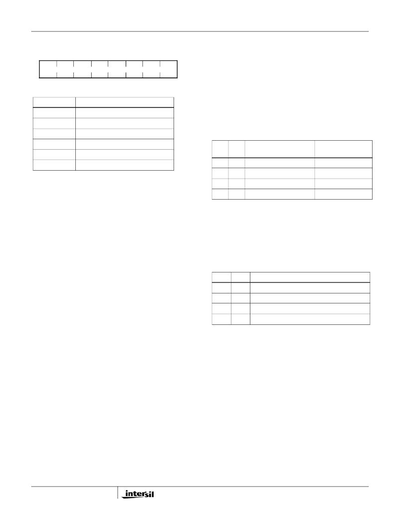
�X9520�
�BL1,� BL0:� BLOCK� LOCK� PROTECTION� BITS� -�
�(NONVOLATILE)�
�CS7�
�POR1�
�CS6�
�V2OS�
�CS5�
�V3OS�
�CS4�
�BL1�
�CS3�
�BL0�
�CS2�
�RWEL�
�CS1�
�WEL�
�CS0�
�POR0�
�The� Block� Lock� protection� bits� (BL1� and� BL0)� are� used� to:�
�?� Inhibit� a� write� operation� from� being� performed� to� certain�
�addresses� of� the� EEPROM� memory� array�
�NV�
�NV�
�NV�
�NV�
�?� Inhibit� a� DCP� write� operation� (changing� the� “wiper�
�position”)�
�BIT(S)�
�WEL�
�RWEL�
�V2OS�
�DESCRIPTION�
�Write� Enable� Latch� bit�
�Register� Write� Enable� Latch� bit�
�V2� Output� Status� flag�
�The� region� of� EEPROM� memory� which� is� protected/locked� is�
�determined� by� the� combination� of� the� BL1� and� BL0� bits�
�written� to� the� CONSTAT� register.� It� is� possible� to� lock� the�
�regions� of� EEPROM� memory� shown� in� the� table� below:�
�V3OS�
�V3� Output� Status� flag�
�PROTECTED� ADDRESSES�
�PARTITION� OF�
�BL1� -� BL0�
�POR1� -� POR0�
�Sets� the� Block� Lock� partition�
�Sets� the� Power-on� Reset� time�
�BL1�
�0�
�BL0�
�0�
�(SIZE)�
�None� (Default)�
�ARRAY� LOCKED�
�None� (Default)�
�NOTE:� Bits� labelled� NV� are� nonvolatile� (See� “CONTROL� AND� STATUS� REGISTER”).�
�FIGURE� 17.� CONSTAT� REGISTER� FORMAT�
�0�
�1�
�1�
�1�
�0�
�1�
�C0h� -� FFh� (64� bytes� )�
�80h� -� FFh� (128� bytes� )�
�00h� -� FFh� (256� bytes)�
�Upper� 1/4�
�Upper� 1/2�
�All�
�DCPs,� EEPROM� array,� as� well� as� the� CONSTAT� register,� is�
�aborted� and� no� ACKNOWLEDGE� is� issued� after� a� Data�
�Byte.�
�The� WEL� bit� is� a� volatile� latch� that� powers� up� in� the� disabled,�
�LOW� (0)� state.� The� WEL� bit� is� enabled/set� by� writing�
�00000010� to� the� CONSTAT� register.� Once� enabled,� the� WEL�
�bit� remains� set� to� “1”� until� either� it� is� reset� to� “0”� (by� writing�
�00000000� to� the� CONSTAT� register)� or� until� the� X9520�
�powers� down,� and� then� up� again.�
�If� the� user� attempts� to� perform� a� write� operation� on� a�
�protected� region� of� EEPROM� memory,� the� operation� is�
�aborted� without� changing� any� data� in� the� array.�
�When� the� Block� Lock� bits� of� the� CONSTAT� register� are� set� to�
�something� other� than� BL1� =� 0� and� BL0� =� 0,� then� the� “wiper�
�position”� of� the� DCPs� cannot� be� changed� -� i.e.� DCP� write�
�operations� cannot� be� conducted:�
�Writes� to� the� WEL� bit� do� not� cause� an� internal� high� voltage�
�write� cycle.� Therefore,� the� device� is� ready� for� another�
�operation� immediately� after� a� STOP� condition� is� executed� in�
�BL1�
�0�
�0�
�BL0�
�0�
�1�
�DCP� WRITE� OPERATION� PERMISSABLE�
�YES� (Default)�
�NO�
�the� CONSTAT� Write� command� sequence� (See� Figure� 18).�
�1�
�0�
�NO�
�RWEL:� REGISTER� WRITE� ENABLE� LATCH� (VOLATILE)�
�1�
�1�
�NO�
�The� RWEL� bit� controls� the� (CONSTAT)� Register� Write�
�Enable� status� of� the� X9520.� Therefore,� in� order� to� write� to�
�any� of� the� bits� of� the� CONSTAT� Register� (except� WEL),� the�
�RWEL� bit� must� first� be� set� to� “1”.� The� RWEL� bit� is� a� volatile�
�bit� that� powers� up� in� the� disabled,� LOW� (“0”)� state.�
�It� must� be� noted� that� the� RWEL� bit� can� only� be� set,� once� the�
�WEL� bit� has� first� been� enabled� (See� "CONSTAT� Register�
�Write� Operation").�
�The� RWEL� bit� will� reset� itself� to� the� default� “0”� state,� in� one�
�of� three� cases:�
�?� After� a� successful� write� operation� to� any� bits� of� the�
�CONSTAT� register� has� been� completed� (See� Figure� 18).�
�?� When� the� X9520� is� powered� down.�
�?� When� attempting� to� write� to� a� Block� Lock� protected� region�
�of� the� EEPROM� memory� (See� "BL1,� BL0:� Block� Lock�
�protection� bits� -� (Nonvolatile)").�
�13�
�The� factory� default� setting� for� these� bits� are� BL1� =� 0,� BL0� =� 0.�
�IMPORTANT� NOTE:� If� the� Write� Protect� (WP)� pin� of� the�
�X9520� is� active� (HIGH),� then� all� nonvolatile� write� operations�
�to� both� the� EEPROM� memory� and� DCPs� are� inhibited,�
�irrespective� of� the� Block� Lock� bit� settings� (See� "WP:� Write�
�Protection� Pin").�
�POR1,� POR0:� POWER-ON� RESET� BITS� –� (NONVOLATILE)�
�Applying� voltage� to� V� CC� activates� the� Power-on� Reset� circuit�
�which� holds� V1RO� output� HIGH,� until� the� supply� voltage�
�stabilizes� above� the� V� TRIP1� threshold� for� a� period� of� time,�
�t� PURST� (See� Figure� 30).�
�The� Power-on� Reset� bits,� POR1� and� POR0� of� the� CONSTAT�
�register� determine� the� t� PURST� delay� time� of� the� Power-on�
�Reset� circuitry� (See� "Voltage� Monitoring� Functions").� These�
�bits� of� the� CONSTAT� register� are� nonvolatile,� and� therefore�
�power-up� to� the� last� written� state.�
�FN8206.2�
�August� 20,� 2007�
�相关PDF资料 |
PDF描述 |
|---|---|
| VE-20V-CX | CONVERTER MOD DC/DC 5.8V 75W |
| CAT28F001HI-12T | IC FLASH MEM 1MBIT 120NS 32TSOP |
| ISL78302AARLLZ-T | IC REG LDO 2.9V .3A 10DFN |
| CAT28F020H90 | IC FLASH MEM 2MBIT 90NS 32TSOP |
| ACM43DRYF | CONN EDGECARD 86POS DIP .156 SLD |
相关代理商/技术参数 |
参数描述 |
|---|---|
| X9520V20I-BT1 | 功能描述:IC VOLT MON DUAL 2KBIT 20-TSSOP RoHS:否 类别:集成电路 (IC) >> PMIC - 激光驱动器 系列:- 产品培训模块:Lead (SnPb) Finish for COTS Obsolescence Mitigation Program 标准包装:60 系列:- 类型:激光二极管驱动器 数据速率:- 通道数:4 电源电压:3.3V 电流 - 电源:- 电流 - 调制:- 电流 - 偏置:- 工作温度:0°C ~ 70°C 封装/外壳:40-TQFN 裸露焊盘 供应商设备封装:40-TQFN EP 包装:托盘 安装类型:表面贴装 |
| X9520V20IZ-A | 制造商:INTERSIL 制造商全称:Intersil Corporation 功能描述:Triple DCP, POR, 2kbit EEPROM Memory, Dual Voltage Monitors |
| X9520V20IZ-AT1 | 制造商:INTERSIL 制造商全称:Intersil Corporation 功能描述:Triple DCP, POR, 2kbit EEPROM Memory, Dual Voltage Monitors |
| X9520V20IZ-AT2 | 制造商:INTERSIL 制造商全称:Intersil Corporation 功能描述:Triple DCP, POR, 2kbit EEPROM Memory, Dual Voltage Monitors |
| X9520V20IZ-B | 制造商:INTERSIL 制造商全称:Intersil Corporation 功能描述:Triple DCP, POR, 2kbit EEPROM Memory, Dual Voltage Monitors |
发布紧急采购,3分钟左右您将得到回复。