参数资料
| 型号: | XA3SD1800A-4FGG676I |
| 厂商: | Xilinx Inc |
| 文件页数: | 12/58页 |
| 文件大小: | 0K |
| 描述: | SPARTAN-3ADSP FPGA 1800K 676FBGA |
| 产品培训模块: | Extended Spartan 3A FPGA Family |
| 标准包装: | 40 |
| 系列: | Spartan®-3A DSP XA |
| LAB/CLB数: | 4160 |
| 逻辑元件/单元数: | 37440 |
| RAM 位总计: | 1548288 |
| 输入/输出数: | 519 |
| 门数: | 1800000 |
| 电源电压: | 1.14 V ~ 1.26 V |
| 安装类型: | 表面贴装 |
| 工作温度: | -40°C ~ 100°C |
| 封装/外壳: | 676-BGA |
| 供应商设备封装: | 676-FBGA(27x27) |
| 配用: | 122-1574-ND - KIT DEVELOPMENT SPARTAN 3ADSP |
第1页第2页第3页第4页第5页第6页第7页第8页第9页第10页第11页当前第12页第13页第14页第15页第16页第17页第18页第19页第20页第21页第22页第23页第24页第25页第26页第27页第28页第29页第30页第31页第32页第33页第34页第35页第36页第37页第38页第39页第40页第41页第42页第43页第44页第45页第46页第47页第48页第49页第50页第51页第52页第53页第54页第55页第56页第57页第58页
XA Spartan-3A DSP Automotive FPGA Family Data Sheet
DS705 (v2.0) April 18, 2011
Product Specification
2
Refer to DS610, Spartan-3A DSP FPGA Family Data Sheet for a full product description, AC and DC specifications, and
package pinout descriptions. Any values shown specifically in this XA Spartan-3A DSP Automotive FPGA Family data sheet
override those shown in DS610.
For information regarding reliability qualification, refer to RPT103, Xilinx Spartan-3A Family Automotive Qualification Report
and RPT070, Spartan-3A Commercial Qualification Report. Contact your local Xilinx representative for more details on
these reports.
Key Feature Differences from Commercial XC Devices
AEC-Q100 device qualification and full production part approval process (PPAP) documentation support available in
both extended temperature I- and Q-Grades
Guaranteed to meet full electrical specifications over the TJ = –40°C to +125°C temperature range (Q-Grade)
XA Spartan-3A DSP devices are available in the -4 speed grade only
PCI-66 and PCI-X are not supported in the XA Spartan-3A DSP FPGA product line
Platform Flash is not supported within the XA family
XA Spartan-3A DSP devices are available in Pb-free packaging only
MultiBoot is not supported in XA versions of this product.
The XA Spartan-3A DSP device must be power cycled prior to reconfiguration.
Architectural Overview
The XA Spartan-3A DSP family architecture consists of five fundamental programmable functional elements:
XtremeDSP DSP48A Slice provides an 18-bit x 18-bit multiplier, 18-bit pre-adder, 48-bit post-adder/accumulator, and
cascade capabilities for various DSP applications.
Configurable Logic Blocks (CLBs) contain flexible Look-Up Tables (LUTs) that implement logic plus storage
elements used as flip-flops or latches. CLBs perform a wide variety of logical functions as well as store data.
Input/Output Blocks (IOBs) control the flow of data between the I/O pins and the internal logic of the device. IOBs
support bidirectional data flow plus 3-state operation. Supports a variety of signal standards, including several
high-performance differential standards. Double Data-Rate (DDR) registers are included.
Block RAM provides data storage in the form of 18-Kb dual-port blocks.
Digital Clock Manager (DCM) Blocks provide self-calibrating, fully digital solutions for distributing, delaying,
multiplying, dividing, and phase-shifting clock signals.
These elements are organized as shown in Figure 1. A dual ring of staggered IOBs surrounds a regular array of CLBs. The
XA3SD1800A has four columns of DSP48A slices, and the XA3SD3400A has five columns of DSP48A slices. Each
DSP48A has an associated block RAM. The DCMs are positioned in the center with two at the top and two at the bottom of
the device and in the two outer columns of the four or five columns of block RAM and DSP48As.
The XA Spartan-3A DSP family features a rich network of routing that interconnect all five functional elements, transmitting
signals among them. Each functional element has an associated switch matrix that permits multiple connections to the
routing.
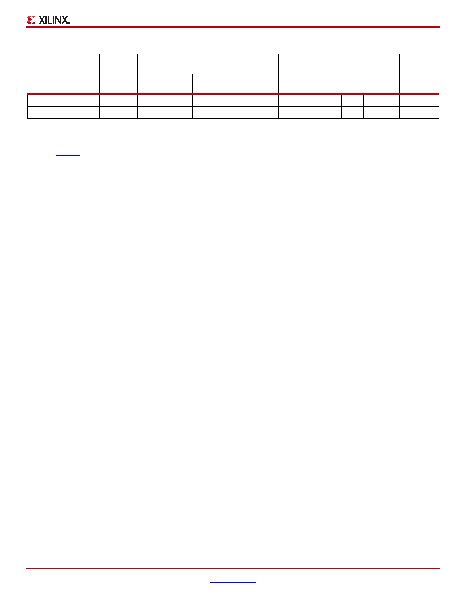
Table 1: Summary of XA Spartan-3A DSP FPGA Attributes
Device
System
Gates
Equivalent
Logic
Cells
CLB Array
(One CLB = Four Slices)
Distributed
RAM bits(1)
Block
RAM
Bits
Dedicated
Multipliers
DCMs
Maximum
User I/O
Maximum
Differential
I/O Pairs
Rows Columns
Total
CLBs
Total
Slices
XA3SD1800A 1800K
37,440
88
48
4,160 16,640
260K
1512K
84
8
519
227
XA3SD3400A 3400K
53,712
104
58
5,968 23,872
373K
2268K
126
8
469
213
Notes:
1.
By convention, one Kb is equivalent to 1,024 bits.
相关PDF资料 |
PDF描述 |
|---|---|
| SST25VF020B-80-4I-QAE | IC FLASH SER 2MB 80MHZ SPI 8WSON |
| XC6SLX75T-3FGG676C | IC FPGA SPARTAN 6 74K 676FGGBGA |
| 24AA256T-I/SM | IC EEPROM 256KBIT 400KHZ 8SOIC |
| XC6SLX100-N3FGG676I | IC FPGA SPARTAN-6 676FBGA |
| 25C160T-E/SN | IC EEPROM 16KBIT 3MHZ 8SOIC |
相关代理商/技术参数 |
参数描述 |
|---|---|
| XA3SD1800A-4FGG676Q | 功能描述:SPARTAN-3ADSP FPGA 1800K 676FBGA RoHS:是 类别:集成电路 (IC) >> 嵌入式 - FPGA(现场可编程门阵列) 系列:Spartan®-3A DSP XA 产品变化通告:Step Intro and Pkg Change 11/March/2008 标准包装:1 系列:Virtex®-5 SXT LAB/CLB数:4080 逻辑元件/单元数:52224 RAM 位总计:4866048 输入/输出数:480 门数:- 电源电压:0.95 V ~ 1.05 V 安装类型:表面贴装 工作温度:-40°C ~ 100°C 封装/外壳:1136-BBGA,FCBGA 供应商设备封装:1136-FCBGA 配用:568-5088-ND - BOARD DEMO DAC1408D750122-1796-ND - EVALUATION PLATFORM VIRTEX-5 |
| XA3SD3400A | 制造商:XILINX 制造商全称:XILINX 功能描述:XA Spartan-3A DSP Automotive FPGA Family Data Sheet |
| XA3SD3400A-4CSG484I | 功能描述:SPARTAN-3ADSP FPGA 3400K 484CSBG RoHS:是 类别:集成电路 (IC) >> 嵌入式 - FPGA(现场可编程门阵列) 系列:Spartan®-3A DSP XA 产品变化通告:Step Intro and Pkg Change 11/March/2008 标准包装:1 系列:Virtex®-5 SXT LAB/CLB数:4080 逻辑元件/单元数:52224 RAM 位总计:4866048 输入/输出数:480 门数:- 电源电压:0.95 V ~ 1.05 V 安装类型:表面贴装 工作温度:-40°C ~ 100°C 封装/外壳:1136-BBGA,FCBGA 供应商设备封装:1136-FCBGA 配用:568-5088-ND - BOARD DEMO DAC1408D750122-1796-ND - EVALUATION PLATFORM VIRTEX-5 |
| XA3SD3400A-4FGG676I | 功能描述:SPARTAN-3ADSP FPGA 3400K 676FBGA RoHS:是 类别:集成电路 (IC) >> 嵌入式 - FPGA(现场可编程门阵列) 系列:Spartan®-3A DSP XA 产品变化通告:Step Intro and Pkg Change 11/March/2008 标准包装:1 系列:Virtex®-5 SXT LAB/CLB数:4080 逻辑元件/单元数:52224 RAM 位总计:4866048 输入/输出数:480 门数:- 电源电压:0.95 V ~ 1.05 V 安装类型:表面贴装 工作温度:-40°C ~ 100°C 封装/外壳:1136-BBGA,FCBGA 供应商设备封装:1136-FCBGA 配用:568-5088-ND - BOARD DEMO DAC1408D750122-1796-ND - EVALUATION PLATFORM VIRTEX-5 |
| X-A4A-300L | 制造商:Leach International Corporation 功能描述:MID RANGE - Bulk |
发布紧急采购,3分钟左右您将得到回复。