参数资料
| 型号: | XA3SD3400A-4CSG484I |
| 厂商: | Xilinx Inc |
| 文件页数: | 33/58页 |
| 文件大小: | 0K |
| 描述: | SPARTAN-3ADSP FPGA 3400K 484CSBG |
| 产品培训模块: | Extended Spartan 3A FPGA Family |
| 标准包装: | 84 |
| 系列: | Spartan®-3A DSP XA |
| LAB/CLB数: | 5968 |
| 逻辑元件/单元数: | 53712 |
| RAM 位总计: | 2322432 |
| 输入/输出数: | 309 |
| 门数: | 3400000 |
| 电源电压: | 1.14 V ~ 1.26 V |
| 安装类型: | 表面贴装 |
| 工作温度: | -40°C ~ 100°C |
| 封装/外壳: | 484-FBGA,CSPBGA |
| 供应商设备封装: | 484-CSPBGA |
第1页第2页第3页第4页第5页第6页第7页第8页第9页第10页第11页第12页第13页第14页第15页第16页第17页第18页第19页第20页第21页第22页第23页第24页第25页第26页第27页第28页第29页第30页第31页第32页当前第33页第34页第35页第36页第37页第38页第39页第40页第41页第42页第43页第44页第45页第46页第47页第48页第49页第50页第51页第52页第53页第54页第55页第56页第57页第58页
XA Spartan-3A DSP Automotive FPGA Family Data Sheet
DS705 (v2.0) April 18, 2011
Product Specification
39
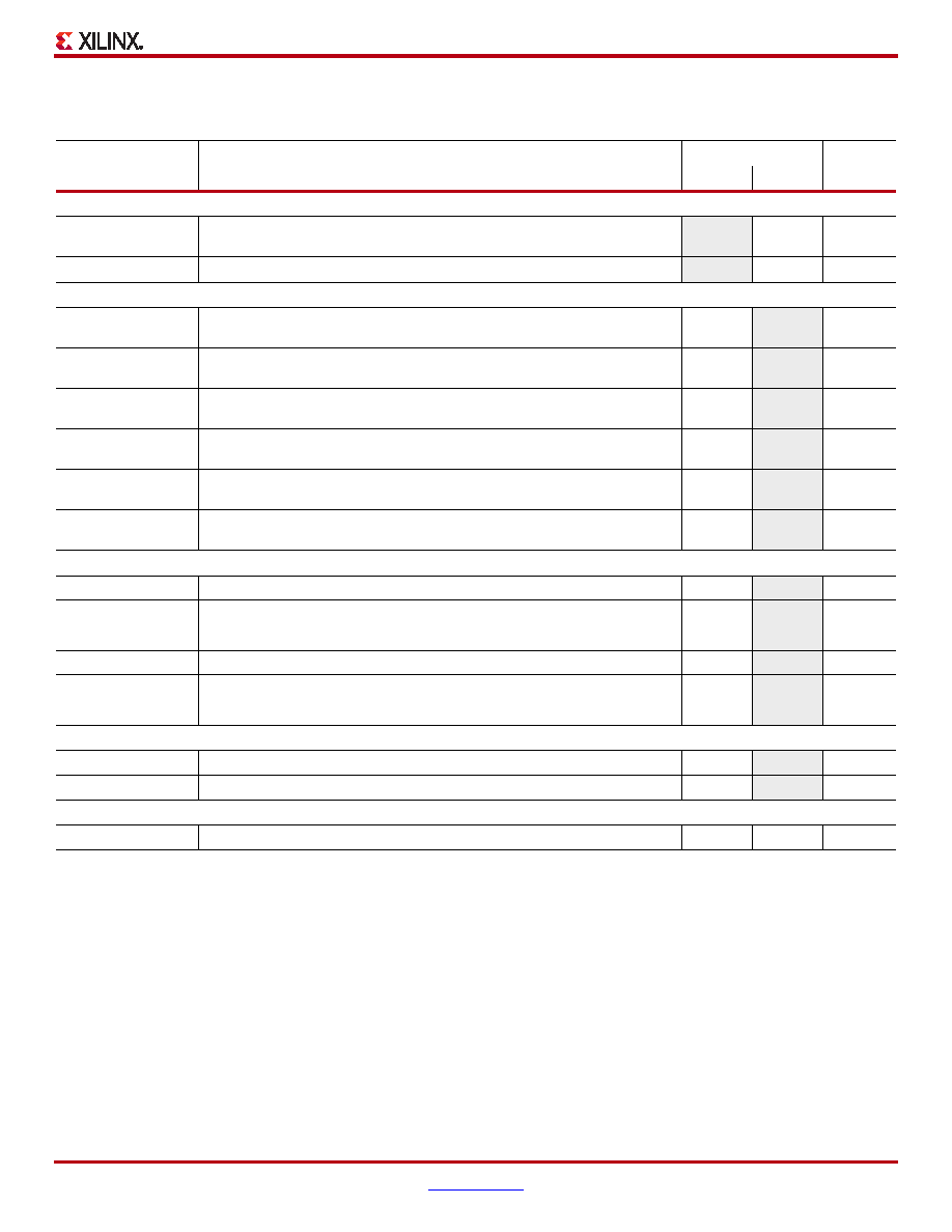
Block RAM Timing
Table 34: Block RAM Timing
Symbol
Description
Speed Grade: -4
Units
Min
Max
Clock-to-Output Times
TRCKO_DOA_NC
When reading from block RAM, the delay from the active transition at the CLK
input to data appearing at the DOUT output
–2.80
ns
TRCKO_DOA
Clock CLK to DOUT output (with output register)
–1.45
ns
Setup Times
TRCCK_ADDR
Setup time for the ADDR inputs before the active transition at the CLK input
of the block RAM
0.46
–ns
TRDCK_DIB
Setup time for data at the DIN inputs before the active transition at the CLK
input of the block RAM
0.33
–ns
TRCCK_ENB
Setup time for the EN input before the active transition at the CLK input of the
block RAM
0.60
–ns
TRCCK_WEB
Setup time for the WE input before the active transition at the CLK input of the
block RAM
0.75
–ns
TRCCK_REGCE
Setup time for the CE input before the active transition at the CLK input of the
block RAM
0.40
–ns
TRCCK_RST
Setup time for the RST input before the active transition at the CLK input of
the block RAM
0.25
–ns
Hold Times
TRCKC_ADDR
Hold time on the ADDR inputs after the active transition at the CLK input
0.10
–ns
TRDCK_DIB
Hold time on the DIN inputs after the active transition at the CLK input
0.10
–ns
TRCKC_ENB
Hold time on the EN input after the active transition at the CLK input
0.10
–ns
TRCKC_WEB
Hold time on the WE input after the active transition at the CLK input
0.10
–ns
TRCKC_REGCE
Hold time on the CE input after the active transition at the CLK input
0.10
–ns
TRCKC_RST
Hold time on the RST input after the active transition at the CLK input
0.10
–ns
Clock Timing
TBPWH
High pulse width of the CLK signal
1.79
–ns
TBPWL
Low pulse width of the CLK signal
1.79
–ns
Clock Frequency
FBRAM
Block RAM clock frequency
0
280
MHz
Notes:
1.
The numbers in this table are based on the operating conditions set forth in Table 8.
相关PDF资料 |
PDF描述 |
|---|---|
| SST25VF080B-80-4I-SAE-T | IC FLASH SER 16MB 80MHZ 8SOIC |
| XC6SLX150-N3FGG676C | IC FPGA SPARTAN-6 676FBGA |
| XC6SLX150-N3FGG484I | IC FPGA SPARTAN-6 484FBGA |
| 24AA256T-I/MF | IC EEPROM CMOS SER 256K 8DFN-S |
| XC6SLX150-N3CSG484I | IC FPGA SPARTAN-6 484CSBGA |
相关代理商/技术参数 |
参数描述 |
|---|---|
| XA3SD3400A-4FGG676I | 功能描述:SPARTAN-3ADSP FPGA 3400K 676FBGA RoHS:是 类别:集成电路 (IC) >> 嵌入式 - FPGA(现场可编程门阵列) 系列:Spartan®-3A DSP XA 产品变化通告:Step Intro and Pkg Change 11/March/2008 标准包装:1 系列:Virtex®-5 SXT LAB/CLB数:4080 逻辑元件/单元数:52224 RAM 位总计:4866048 输入/输出数:480 门数:- 电源电压:0.95 V ~ 1.05 V 安装类型:表面贴装 工作温度:-40°C ~ 100°C 封装/外壳:1136-BBGA,FCBGA 供应商设备封装:1136-FCBGA 配用:568-5088-ND - BOARD DEMO DAC1408D750122-1796-ND - EVALUATION PLATFORM VIRTEX-5 |
| X-A4A-300L | 制造商:Leach International Corporation 功能描述:MID RANGE - Bulk |
| X-A4C-300M | 制造商:Leach International Corporation 功能描述:MID RANGE - Bulk |
| X-A4M-300L | 制造商:Leach International Corporation 功能描述:MID RANGE - Bulk |
| X-A4M-300M | 制造商:Leach International Corporation 功能描述:MID RANGE - Bulk |
发布紧急采购,3分钟左右您将得到回复。