参数资料
| 型号: | XC2S100E-6FTG256C |
| 厂商: | Xilinx Inc |
| 文件页数: | 62/108页 |
| 文件大小: | 0K |
| 描述: | IC SPARTAN-IIE FPGA 100K 256FBGA |
| 产品变化通告: | FPGA Family Discontinuation 18/Apr/2011 |
| 标准包装: | 90 |
| 系列: | Spartan®-IIE |
| LAB/CLB数: | 600 |
| 逻辑元件/单元数: | 2700 |
| RAM 位总计: | 40960 |
| 输入/输出数: | 182 |
| 门数: | 100000 |
| 电源电压: | 1.71 V ~ 1.89 V |
| 安装类型: | 表面贴装 |
| 工作温度: | 0°C ~ 85°C |
| 封装/外壳: | 256-LBGA |
| 供应商设备封装: | 256-FTBGA |
| 其它名称: | 122-1322 |
第1页第2页第3页第4页第5页第6页第7页第8页第9页第10页第11页第12页第13页第14页第15页第16页第17页第18页第19页第20页第21页第22页第23页第24页第25页第26页第27页第28页第29页第30页第31页第32页第33页第34页第35页第36页第37页第38页第39页第40页第41页第42页第43页第44页第45页第46页第47页第48页第49页第50页第51页第52页第53页第54页第55页第56页第57页第58页第59页第60页第61页当前第62页第63页第64页第65页第66页第67页第68页第69页第70页第71页第72页第73页第74页第75页第76页第77页第78页第79页第80页第81页第82页第83页第84页第85页第86页第87页第88页第89页第90页第91页第92页第93页第94页第95页第96页第97页第98页第99页第100页第101页第102页第103页第104页第105页第106页第107页第108页
DS077-4 (v3.0) August 9, 2013
57
Product Specification
Spartan-IIE FPGA Family: Pinout Tables
R
— OBSOLETE — OBSOLETE — OBSOLETE — OBSOLETE —
Low Voltage Differential Signals (LVDS
and LVPECL)
The Spartan-IIE family features low-voltage differential sig-
naling (LVDS and LVPECL). Each signal utilizes two pins on
the Spartan-IIE device, known as differential pin pairs. Each
differential pin pair has a Positive (P) and a Negative (N) pin.
These pairs are labeled in the following manner.
I/O, L#[P/N][-/_Y/_YY]
where
L = LVDS or LVPECL pin
# = Pin pair number
P = Positive
N = Negative
_Y = Asynchronous output allowed (device-dependent)
_YY = Asynchronous output allowed (all devices)
Synchronous or Asynchronous
I/O pins for differential signals can either be synchronous or
asynchronous,
input
or
output.
Differential
signaling
requires the pins of each pair to switch simultaneously. If the
output signals driving the pins are from IOB flip-flops, they
are synchronous. If the signals driving the pins are from
internal logic, they are asynchronous, and therefore more
care must be taken that they are simultaneous. Any differ-
ential pairs can be used for synchronous input and output
signals as well as asynchronous input signals.
However, only the differential pairs with the _Y or _YY suffix
can be used for asynchronous output signals.
Asynchronous Output Pad Name Designation
Because of differences between densities, the differential
pairs that can be used for asynchronous outputs vary by
device. The pairs that are available in all densities for a
given package have the _YY suffix. These pins should be
used for differential asynchronous outputs if the design may
later move to a different density. All other differential pairs
that can be used for asynchronous outputs have the _Y suf-
fix.
To simplify the following tables, the "Pad Name" column
shows the part of the name that is common across densi-
ties. The "Pad Name" column leaves out the _Y suffix and
the "LVDS Asynchronous Output Option" column indicates
the densities that allow asynchronous outputs for LVDS or
LVPECL on the given pin.
DLL Pins
Pins labeled "I/O (DLL)" can be used as general-purpose
I/O or as inputs to the DLL. Adjacent DLL pins form a differ-
ential pair. They reside in two different banks, so if they are
outputs the VCCO level must be the same for both banks.
Each DLL pin can also be paired with the adjacent GCK
clock pin for a differential clock input. The "I/O (DLL)" pin
always becomes the N terminal when paired with GCK,
even if it is labeled "P" for its pairing with the adjacent DLL
pin.
VREF Pins
Pins labeled "I/O, VREF" can be used as either an I/O or a
VREF pin. If any I/O pin within the bank requires a VREF
input, all the VREF pins in the bank must be connected to
the same voltage. See the I/O banking rules in the Func-
tional Description module for more detail. If no pin in a
given bank requires VREF, then that bank's VREF pins can
be used as general I/O.
To simplify the following tables, the "Pad Name" column
shows the part of the name that is common across densi-
ties. When VREF is only available in limited densities, the
"Pad Name" column leaves out the VREF designation and
the "VREF Option" column indicates the densities that pro-
vide VREF on the given pin.
VCCO Banks
In the TQ144 and PQ208 packages, the eight banks have
VCCO connected together. Thus, only one VCCO is
allowed in these packages, although different VREF values
are allowed in each of the eight banks. See I/O Banking.
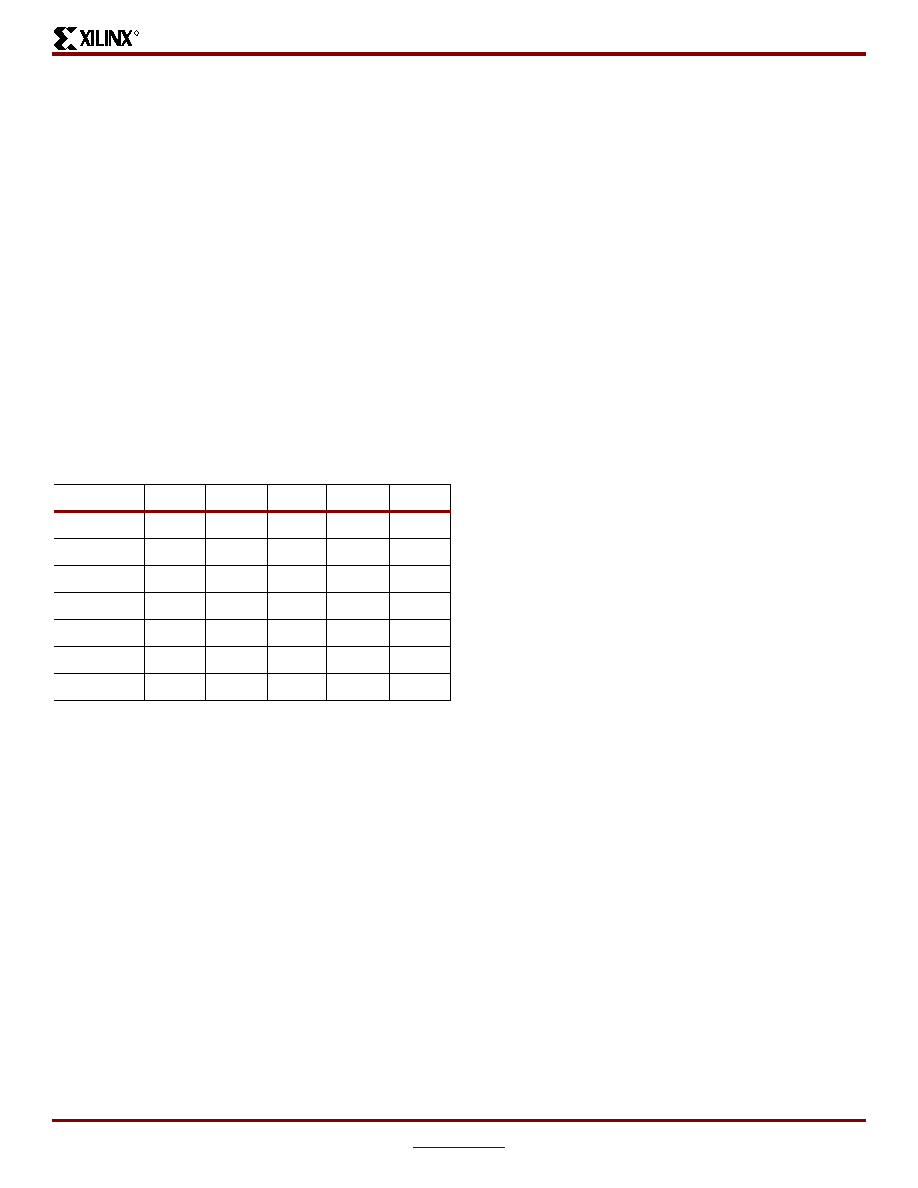
Available Differential Pairs According to
Package Type
Device
TQ144
PQ208
FT256
FG456
FG676
XC2S50E
28
50
83
-
XC2S100E
28
50
83
86
-
XC2S150E
-
50
83
114
-
XC2S200E
-
50
83
120
-
XC2S300E
-
50
83
120
-
XC2S400E
-
83
120
172
XC2S600E
-
120
205
相关PDF资料 |
PDF描述 |
|---|---|
| ACB91DHFT-S621 | EDGECARD 182POS SMD W/O POST |
| ABB91DHFT-S621 | EDGECARD 182PS .050 SMD W/O POST |
| ACB91DHFT-S578 | EDGECARD 182POS .050 SMD W/POSTS |
| XC2S100E-6FT256C | IC FPGA 1.8V 600 CLB'S 256-FBGA |
| ABB91DHFT-S578 | EDGECARD 182POS .050 SMD W/POSTS |
相关代理商/技术参数 |
参数描述 |
|---|---|
| XC2S100E-6FTG256I | 制造商:XILINX 制造商全称:XILINX 功能描述:Spartan-IIE FPGA |
| XC2S100E-6PQ208C | 功能描述:IC FPGA 1.8V 600 CLB'S 208-PQFP RoHS:否 类别:集成电路 (IC) >> 嵌入式 - FPGA(现场可编程门阵列) 系列:Spartan®-IIE 标准包装:40 系列:Spartan® 6 LX LAB/CLB数:3411 逻辑元件/单元数:43661 RAM 位总计:2138112 输入/输出数:358 门数:- 电源电压:1.14 V ~ 1.26 V 安装类型:表面贴装 工作温度:-40°C ~ 100°C 封装/外壳:676-BGA 供应商设备封装:676-FBGA(27x27) |
| XC2S100E-6PQ208I | 制造商:XILINX 制造商全称:XILINX 功能描述:Spartan-IIE FPGA |
| XC2S100E-6PQG208C | 功能描述:IC FPGA 1.8V 600 CLB'S 208-PQFP RoHS:是 类别:集成电路 (IC) >> 嵌入式 - FPGA(现场可编程门阵列) 系列:Spartan®-IIE 标准包装:40 系列:Spartan® 6 LX LAB/CLB数:3411 逻辑元件/单元数:43661 RAM 位总计:2138112 输入/输出数:358 门数:- 电源电压:1.14 V ~ 1.26 V 安装类型:表面贴装 工作温度:-40°C ~ 100°C 封装/外壳:676-BGA 供应商设备封装:676-FBGA(27x27) |
| XC2S100E-6PQG208I | 制造商:XILINX 制造商全称:XILINX 功能描述:Spartan-IIE FPGA |
发布紧急采购,3分钟左右您将得到回复。