参数资料
| 型号: | XC2S30-5PQ208C |
| 厂商: | Xilinx Inc |
| 文件页数: | 49/99页 |
| 文件大小: | 0K |
| 描述: | IC FPGA 2.5V 216 CLB'S 208-PQFP |
| 标准包装: | 24 |
| 系列: | Spartan®-II |
| LAB/CLB数: | 216 |
| 逻辑元件/单元数: | 972 |
| RAM 位总计: | 24576 |
| 输入/输出数: | 140 |
| 门数: | 30000 |
| 电源电压: | 2.375 V ~ 2.625 V |
| 安装类型: | 表面贴装 |
| 工作温度: | 0°C ~ 85°C |
| 封装/外壳: | 208-BFQFP |
| 供应商设备封装: | 208-PQFP(28x28) |
| 其它名称: | 122-1220 XC2S30-5PQ208C-ND |
第1页第2页第3页第4页第5页第6页第7页第8页第9页第10页第11页第12页第13页第14页第15页第16页第17页第18页第19页第20页第21页第22页第23页第24页第25页第26页第27页第28页第29页第30页第31页第32页第33页第34页第35页第36页第37页第38页第39页第40页第41页第42页第43页第44页第45页第46页第47页第48页当前第49页第50页第51页第52页第53页第54页第55页第56页第57页第58页第59页第60页第61页第62页第63页第64页第65页第66页第67页第68页第69页第70页第71页第72页第73页第74页第75页第76页第77页第78页第79页第80页第81页第82页第83页第84页第85页第86页第87页第88页第89页第90页第91页第92页第93页第94页第95页第96页第97页第98页第99页
Spartan-II FPGA Family: DC and Switching Characteristics
DS001-3 (v2.8) June 13, 2008
Module 3 of 4
Product Specification
53
R
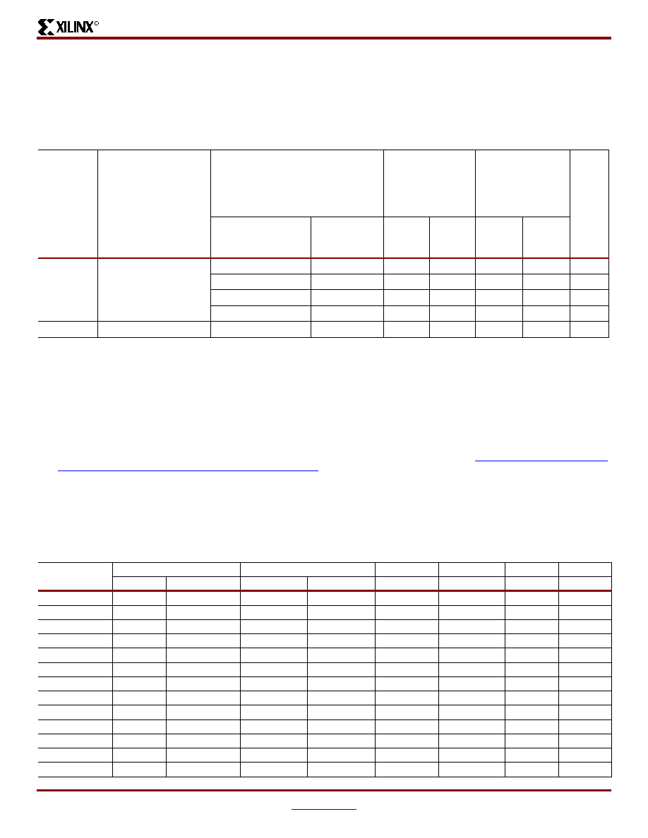
Power-On Requirements
Spartan-II FPGAs require that a minimum supply current
ICCPO be provided to the VCCINT lines for a successful
power-on. If more current is available, the FPGA can
consume more than ICCPO minimum, though this cannot
adversely affect reliability.
A maximum limit for ICCPO is not specified. Therefore the
use of foldback/crowbar supplies and fuses deserves
special attention. In these cases, limit the ICCPO current to a
level below the trip point for over-current protection in order
to avoid inadvertently shutting down the supply.
DC Input and Output Levels
Values for VIL and VIH are recommended input voltages.
Values for VOL and VOH are guaranteed output voltages
over the recommended operating conditions. Only selected
standards are tested. These are chosen to ensure that all
standards meet their specifications. The selected standards
are tested at minimum VCCO with the respective IOL and IOH
currents shown. Other standards are sample tested.
Symbol
Description
Conditions
New
Requirements(1)
For Devices with
Date Code 0321
or Later
Old
Requirements(1)
For Devices with
Date Code
before 0321
Units
Junction
Temperature(2)
Device
Temperature
Grade
Min
Max
Min
Max
I CCPO(3)
Total VCCINT supply
current required
during power-on
–40°C
≤ TJ<–20°C
Industrial
1.50
-
2.00
-
A
–20°C
≤ TJ < 0°C
Industrial
1.00
-
2.00
-
A
0°C
≤ TJ ≤ 85°C
Commercial
0.25
-
0.50
-
A
85°C < TJ ≤ 100°C
Industrial
0.50
-
0.50
-
A
TCCPO(4,5) VCCINT ramp time
–40°C
≤ TJ≤ 100°C
All
-
50
-
50
ms
Notes:
1.
The date code is printed on the top of the device’s package. See the "Device Part Marking" section in Module 1.
2.
The expected TJ range for the design determines the ICCPO minimum requirement. Use the applicable ranges in the junction
temperature column to find the associated current values in the appropriate new or old requirements column according to the date
code. Then choose the highest of these current values to serve as the minimum ICCPO requirement that must be met. For example,
if the junction temperature for a given design is -25°C
≤ TJ ≤ 75°C, then the new minimum ICCPO requirement is 1.5A.
If 5°C
≤ TJ ≤ 90°C, then the new minimum ICCPO requirement is 0.5A.
3.
The ICCPO requirement applies for a brief time (commonly only a few milliseconds) when VCCINT ramps from 0 to 2.5V.
4.
The ramp time is measured from GND to VCCINT max on a fully loaded board.
5.
During power-on, the VCCINT ramp must increase steadily in voltage with no dips.
6.
For more information on designing to meet the power-on specifications, refer to the application note XAPP450 "Power-On Current
Input/Output
Standard
VIL
VIH
VOL
VOH
IOL
IOH
V, Min
V, Max
V, Min
V, Max
V, Min
mA
LVTTL(1)
–0.5
0.8
2.0
5.5
0.4
2.4
24
–24
LVCMOS2
–0.5
0.7
1.7
5.5
0.4
1.9
12
–12
PCI, 3.3V
–0.5
44% VCCINT
60% VCCINT
VCCO + 0.5
10% VCCO
90% VCCO
Note (2)
PCI, 5.0V
–0.5
0.8
2.0
5.5
0.55
2.4
Note (2)
GTL
–0.5
VREF – 0.05
VREF + 0.05
3.6
0.4
N/A
40
N/A
GTL+
–0.5
VREF – 0.1
VREF + 0.1
3.6
0.6
N/A
36
N/A
HSTL I
–0.5
VREF – 0.1
VREF + 0.1
3.6
0.4
VCCO – 0.4
8
–8
HSTL III
–0.5
VREF – 0.1
VREF + 0.1
3.6
0.4
VCCO – 0.4
24
–8
HSTL IV
–0.5
VREF – 0.1
VREF + 0.1
3.6
0.4
VCCO – 0.4
48
–8
SSTL3 I
–0.5
VREF – 0.2
VREF + 0.2
3.6
VREF – 0.6
VREF + 0.6
8
–8
SSTL3 II
–0.5
VREF – 0.2
VREF + 0.2
3.6
VREF – 0.8
VREF + 0.8
16
–16
SSTL2 I
–0.5
VREF – 0.2
VREF + 0.2
3.6
VREF – 0.6
VREF + 0.6
7.6
–7.6
SSTL2 II
–0.5
VREF – 0.2
VREF + 0.2
3.6
VREF – 0.8
VREF + 0.8
15.2
–15.2
相关PDF资料 |
PDF描述 |
|---|---|
| XC2S15-6CS144C | IC FPGA 2.5V C-TEMP 144-CSBGA |
| XC2S15-5CS144I | IC FPGA 2.5V I-TEMP 144-CSBGA |
| XC2S15-5CS144C | IC FPGA 2.5V C-TEMP 144-CSBGA |
| XC2S100-5FG456I | IC FPGA 2.5V I-TEMP 456-FBGA |
| IDT71V35761S183PFG | IC SRAM 4MBIT 183MHZ 100TQFP |
相关代理商/技术参数 |
参数描述 |
|---|---|
| XC2S30-5PQ208I | 功能描述:IC FPGA 2.5V I-TEMP 208-PQFP RoHS:否 类别:集成电路 (IC) >> 嵌入式 - FPGA(现场可编程门阵列) 系列:Spartan®-II 产品变化通告:XC4000(E,L) Discontinuation 01/April/2002 标准包装:24 系列:XC4000E/X LAB/CLB数:100 逻辑元件/单元数:238 RAM 位总计:3200 输入/输出数:80 门数:3000 电源电压:4.5 V ~ 5.5 V 安装类型:表面贴装 工作温度:-40°C ~ 100°C 封装/外壳:120-BCBGA 供应商设备封装:120-CPGA(34.55x34.55) |
| XC2S30-5PQG208C | 制造商:XILINX 制造商全称:XILINX 功能描述:Spartan-II FPGA Family |
| XC2S30-5PQG208I | 制造商:XILINX 制造商全称:XILINX 功能描述:Spartan-II FPGA Family |
| XC2S305TQ144C | 制造商:XILINX 功能描述:New |
| XC2S30-5TQ144C | 功能描述:IC FPGA 2.5V 216 CLB'S 144-TQFP RoHS:否 类别:集成电路 (IC) >> 嵌入式 - FPGA(现场可编程门阵列) 系列:Spartan®-II 标准包装:40 系列:Spartan® 6 LX LAB/CLB数:3411 逻辑元件/单元数:43661 RAM 位总计:2138112 输入/输出数:358 门数:- 电源电压:1.14 V ~ 1.26 V 安装类型:表面贴装 工作温度:-40°C ~ 100°C 封装/外壳:676-BGA 供应商设备封装:676-FBGA(27x27) |
发布紧急采购,3分钟左右您将得到回复。