参数资料
| 型号: | XC2V40-5FGG256C |
| 厂商: | Xilinx Inc |
| 文件页数: | 247/318页 |
| 文件大小: | 0K |
| 描述: | IC FPGA VIRTEX-II 40K 256-FBGA |
| 产品变化通告: | FPGA Family Discontinuation 18/Apr/2011 |
| 标准包装: | 90 |
| 系列: | Virtex®-II |
| LAB/CLB数: | 64 |
| RAM 位总计: | 73728 |
| 输入/输出数: | 88 |
| 门数: | 40000 |
| 电源电压: | 1.425 V ~ 1.575 V |
| 安装类型: | 表面贴装 |
| 工作温度: | 0°C ~ 85°C |
| 封装/外壳: | 256-BGA |
| 供应商设备封装: | 256-FBGA(17x17) |
第1页第2页第3页第4页第5页第6页第7页第8页第9页第10页第11页第12页第13页第14页第15页第16页第17页第18页第19页第20页第21页第22页第23页第24页第25页第26页第27页第28页第29页第30页第31页第32页第33页第34页第35页第36页第37页第38页第39页第40页第41页第42页第43页第44页第45页第46页第47页第48页第49页第50页第51页第52页第53页第54页第55页第56页第57页第58页第59页第60页第61页第62页第63页第64页第65页第66页第67页第68页第69页第70页第71页第72页第73页第74页第75页第76页第77页第78页第79页第80页第81页第82页第83页第84页第85页第86页第87页第88页第89页第90页第91页第92页第93页第94页第95页第96页第97页第98页第99页第100页第101页第102页第103页第104页第105页第106页第107页第108页第109页第110页第111页第112页第113页第114页第115页第116页第117页第118页第119页第120页第121页第122页第123页第124页第125页第126页第127页第128页第129页第130页第131页第132页第133页第134页第135页第136页第137页第138页第139页第140页第141页第142页第143页第144页第145页第146页第147页第148页第149页第150页第151页第152页第153页第154页第155页第156页第157页第158页第159页第160页第161页第162页第163页第164页第165页第166页第167页第168页第169页第170页第171页第172页第173页第174页第175页第176页第177页第178页第179页第180页第181页第182页第183页第184页第185页第186页第187页第188页第189页第190页第191页第192页第193页第194页第195页第196页第197页第198页第199页第200页第201页第202页第203页第204页第205页第206页第207页第208页第209页第210页第211页第212页第213页第214页第215页第216页第217页第218页第219页第220页第221页第222页第223页第224页第225页第226页第227页第228页第229页第230页第231页第232页第233页第234页第235页第236页第237页第238页第239页第240页第241页第242页第243页第244页第245页第246页当前第247页第248页第249页第250页第251页第252页第253页第254页第255页第256页第257页第258页第259页第260页第261页第262页第263页第264页第265页第266页第267页第268页第269页第270页第271页第272页第273页第274页第275页第276页第277页第278页第279页第280页第281页第282页第283页第284页第285页第286页第287页第288页第289页第290页第291页第292页第293页第294页第295页第296页第297页第298页第299页第300页第301页第302页第303页第304页第305页第306页第307页第308页第309页第310页第311页第312页第313页第314页第315页第316页第317页第318页
Virtex-II Platform FPGAs: Functional Description
R
DS031-2 (v3.5) November 5, 2007
Module 2 of 4
Product Specification
26
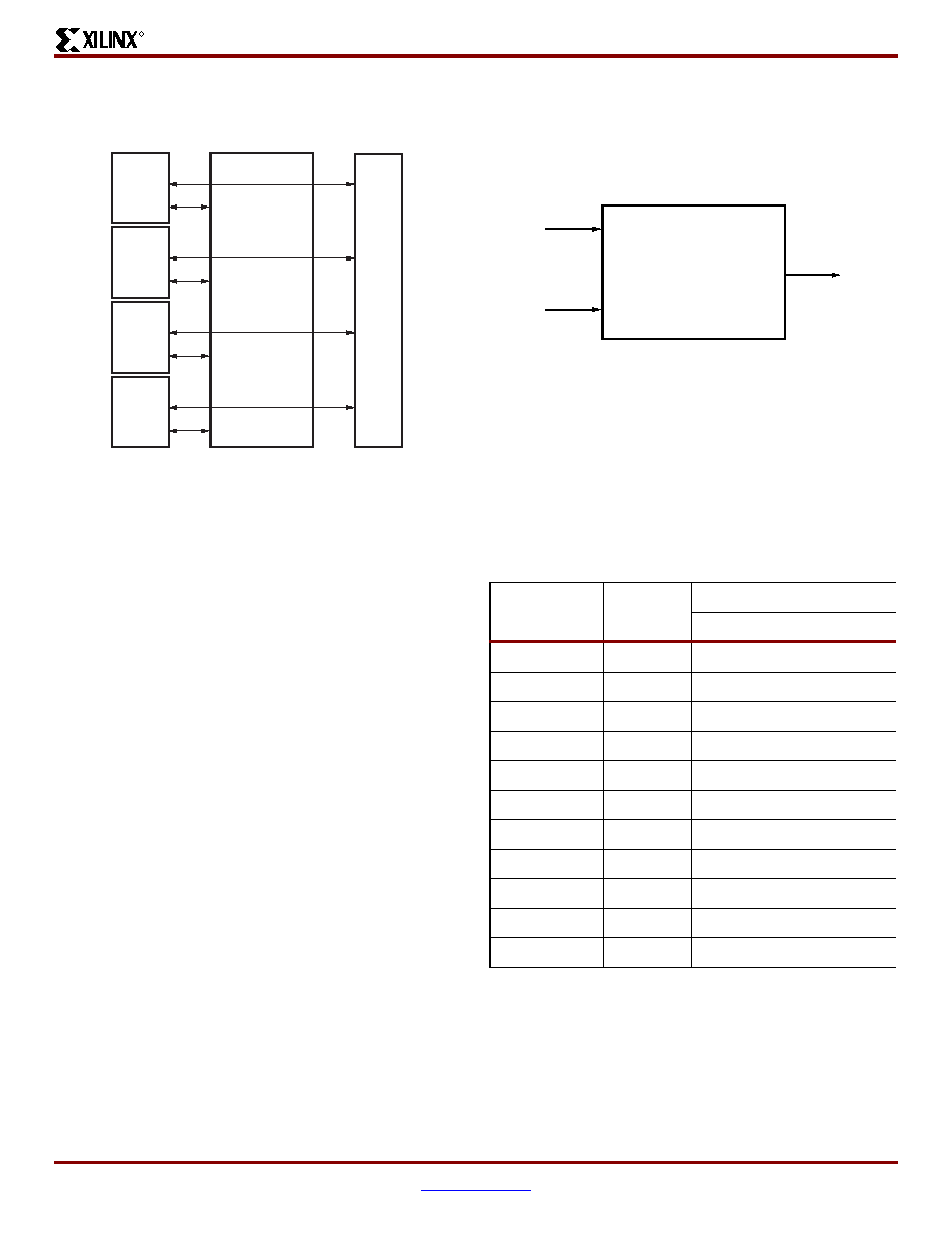
Each SelectRAM memory and multiplier block is tied to four
switch matrices, as shown in Figure 35.
Association With Block SelectRAM Memory
The interconnect is designed to allow SelectRAM memory
and multiplier blocks to be used at the same time, but some
interconnect is shared between the SelectRAM and the
multiplier. Thus, SelectRAM memory can be used only up to
18 bits wide when the multiplier is used, because the multi-
plier shares inputs with the upper data bits of the
SelectRAM memory.
This sharing of the interconnect is optimized for an
18-bit-wide block SelectRAM resource feeding the multi-
plier. The use of SelectRAM memory and the multiplier with
an accumulator in LUTs allows for implementation of a digi-
tal signal processor (DSP) multiplier-accumulator (MAC)
function, which is commonly used in finite and infinite
impulse response (FIR and IIR) digital filters.
Configuration
The multiplier block is an 18-bit by 18-bit signed multiplier
(2's complement). Both A and B are 18-bit-wide inputs, and
the output is 36 bits. Figure 36 shows a multiplier block.
Locations / Organization
Multiplier organization is identical to the 18 Kbit SelectRAM
organization, because each multiplier is associated with an
18 Kbit block SelectRAM resource.
In addition to the built-in multiplier blocks, the CLB elements
have dedicated logic to implement efficient multipliers in
logic. (Refer to Configurable Logic Blocks (CLBs)).
Figure 35: SelectRAM and Multiplier Blocks
Switch
Matrix
Switch
Matrix
18-Kbit block
SelectRAM
18
x
18
Multiplier
Switch
Matrix
Switch
Matrix
DS031_33_101000
Figure 36: Multiplier Block
Table 20: Multiplier Floor Plan
Device
Columns
Multipliers
Per Column
Total
XC2V40
2
4
XC2V80
2
4
8
XC2V250
4
6
24
XC2V500
4
8
32
XC2V1000
4
10
40
XC2V1500
4
12
48
XC2V2000
4
14
56
XC2V3000
6
16
96
XC2V4000
6
20
120
XC2V6000
6
24
144
XC2V8000
6
28
168
MULT 18 x 18
A[17:0]
P[35:0]
B[17:0]
Multiplier Block
DS031_40_100400
相关PDF资料 |
PDF描述 |
|---|---|
| XC2V40-4FGG256I | IC FPGA VIRTEX-II 40K 256-FBGA |
| 3341-32BULK | CONN JACKSOCKET M2.5/4-40 0.50" |
| DB53750-2 | DSUB DB INTERFACIAL SEAL |
| XC3S1400A-5FTG256C | IC FPGA SPARTAN3A 1400K 256FTBGA |
| XC6SLX25-2FGG484C | IC FPGA SPARTAN 6 24K 484FGGBGA |
相关代理商/技术参数 |
参数描述 |
|---|---|
| XC2V40-5FGG256I | 功能描述:IC FPGA VIRTEX-II 40K 256-FBGA RoHS:是 类别:集成电路 (IC) >> 嵌入式 - FPGA(现场可编程门阵列) 系列:Virtex®-II 标准包装:40 系列:Spartan® 6 LX LAB/CLB数:3411 逻辑元件/单元数:43661 RAM 位总计:2138112 输入/输出数:358 门数:- 电源电压:1.14 V ~ 1.26 V 安装类型:表面贴装 工作温度:-40°C ~ 100°C 封装/外壳:676-BGA 供应商设备封装:676-FBGA(27x27) |
| XC2V40-6BF957C | 制造商:XILINX 制造商全称:XILINX 功能描述:Virtex-II 1.5V Field-Programmable Gate Arrays |
| XC2V40-6BF957I | 制造商:XILINX 制造商全称:XILINX 功能描述:Virtex-II 1.5V Field-Programmable Gate Arrays |
| XC2V40-6BG575C | 制造商:XILINX 制造商全称:XILINX 功能描述:Virtex-II 1.5V Field-Programmable Gate Arrays |
| XC2V40-6BG575I | 制造商:XILINX 制造商全称:XILINX 功能描述:Virtex-II 1.5V Field-Programmable Gate Arrays |
发布紧急采购,3分钟左右您将得到回复。