参数资料
| 型号: | XC2V40-5FGG256C |
| 厂商: | Xilinx Inc |
| 文件页数: | 250/318页 |
| 文件大小: | 0K |
| 描述: | IC FPGA VIRTEX-II 40K 256-FBGA |
| 产品变化通告: | FPGA Family Discontinuation 18/Apr/2011 |
| 标准包装: | 90 |
| 系列: | Virtex®-II |
| LAB/CLB数: | 64 |
| RAM 位总计: | 73728 |
| 输入/输出数: | 88 |
| 门数: | 40000 |
| 电源电压: | 1.425 V ~ 1.575 V |
| 安装类型: | 表面贴装 |
| 工作温度: | 0°C ~ 85°C |
| 封装/外壳: | 256-BGA |
| 供应商设备封装: | 256-FBGA(17x17) |
第1页第2页第3页第4页第5页第6页第7页第8页第9页第10页第11页第12页第13页第14页第15页第16页第17页第18页第19页第20页第21页第22页第23页第24页第25页第26页第27页第28页第29页第30页第31页第32页第33页第34页第35页第36页第37页第38页第39页第40页第41页第42页第43页第44页第45页第46页第47页第48页第49页第50页第51页第52页第53页第54页第55页第56页第57页第58页第59页第60页第61页第62页第63页第64页第65页第66页第67页第68页第69页第70页第71页第72页第73页第74页第75页第76页第77页第78页第79页第80页第81页第82页第83页第84页第85页第86页第87页第88页第89页第90页第91页第92页第93页第94页第95页第96页第97页第98页第99页第100页第101页第102页第103页第104页第105页第106页第107页第108页第109页第110页第111页第112页第113页第114页第115页第116页第117页第118页第119页第120页第121页第122页第123页第124页第125页第126页第127页第128页第129页第130页第131页第132页第133页第134页第135页第136页第137页第138页第139页第140页第141页第142页第143页第144页第145页第146页第147页第148页第149页第150页第151页第152页第153页第154页第155页第156页第157页第158页第159页第160页第161页第162页第163页第164页第165页第166页第167页第168页第169页第170页第171页第172页第173页第174页第175页第176页第177页第178页第179页第180页第181页第182页第183页第184页第185页第186页第187页第188页第189页第190页第191页第192页第193页第194页第195页第196页第197页第198页第199页第200页第201页第202页第203页第204页第205页第206页第207页第208页第209页第210页第211页第212页第213页第214页第215页第216页第217页第218页第219页第220页第221页第222页第223页第224页第225页第226页第227页第228页第229页第230页第231页第232页第233页第234页第235页第236页第237页第238页第239页第240页第241页第242页第243页第244页第245页第246页第247页第248页第249页当前第250页第251页第252页第253页第254页第255页第256页第257页第258页第259页第260页第261页第262页第263页第264页第265页第266页第267页第268页第269页第270页第271页第272页第273页第274页第275页第276页第277页第278页第279页第280页第281页第282页第283页第284页第285页第286页第287页第288页第289页第290页第291页第292页第293页第294页第295页第296页第297页第298页第299页第300页第301页第302页第303页第304页第305页第306页第307页第308页第309页第310页第311页第312页第313页第314页第315页第316页第317页第318页
Virtex-II Platform FPGAs: Functional Description
R
DS031-2 (v3.5) November 5, 2007
Module 2 of 4
Product Specification
29
If the CE input is inactive (Low) prior to the incoming rising
clock edge, the following clock pulse does not pass through
the clock buffer, and the output stays Low. Any level change
of CE during the incoming clock High time has no effect. CE
must not change during a short setup window just prior to
the rising clock edge on the BUFGCE input I. Violating this
setup time requirement can result in an undefined runt
pulse output.
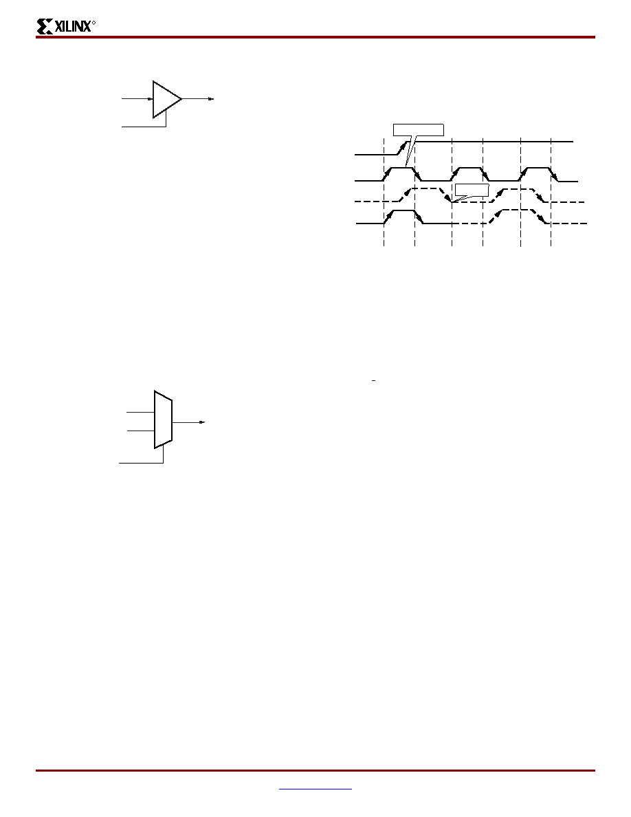
BUFGMUX
BUFGMUX can switch between two unrelated, even asyn-
chronous clocks. Basically, a Low on S selects the I0 input,
a High on S selects the I1 input. Switching from one clock to
the other is done in such a way that the output High and Low
time is never shorter than the shortest High or Low time of
either input clock. As long as the presently selected clock is
High, any level change of S has no effect .
If the presently selected clock is Low while S changes, or if
it goes Low after S has changed, the output is kept Low until
the other ("to-be-selected") clock has made a transition
from High to Low. At that instant, the new clock starts driv-
ing the output.
The two clock inputs can be asynchronous with regard to
each other, and the S input can change at any time, except
for a short setup time prior to the rising edge of the presently
selected clock (I0 or I1). Violating this setup time require-
ment can result in an undefined runt pulse output.
All Virtex-II devices have 16 global clock multiplexer buffers.
Figure 44 shows a switchover from I0 to I1.
The current clock is CLK0.
S is activated High.
If CLK0 is currently High, the multiplexer waits for CLK0
to go Low.
Once CLK0 is Low, the multiplexer output stays Low
until CLK1 transitions High to Low.
When CLK1 transitions from High to Low, the output
switches to CLK1.
No glitches or short pulses can appear on the output.
Local Clocking
In addition to global clocks, there are local clock resources
in the Virtex-II devices. There are more than 72 local clocks
in the Virtex-II family. These resources can be used for
many different applications, including but not limited to
memory interfaces. For example, even using only the left
and right I/O banks, Virtex-II FPGAs can support up to 50
local clocks for DDR SDRAM. These interfaces can operate
beyond 200 MHz on Virtex-II devices.
Digital Clock Manager (DCM)
The Virtex-II DCM offers a wide range of powerful clock
management features.
Clock De-skew: The DCM generates new system
clocks (either internally or externally to the FPGA),
which are phase-aligned to the input clock, thus
eliminating clock distribution delays.
Frequency Synthesis: The DCM generates a wide
range of output clock frequencies, performing very
flexible clock multiplication and division.
Phase Shifting: The DCM provides both coarse phase
shifting and fine-grained phase shifting with dynamic
phase shift control.
The DCM utilizes fully digital delay lines allowing robust
high-precision control of clock phase and frequency. It also
utilizes fully digital feedback systems, operating dynamically
to compensate for temperature and voltage variations dur-
ing operation.
Up to four of the nine DCM clock outputs can drive inputs to
global clock buffers or global clock multiplexer buffers simul-
taneously (see Figure 45). All DCM clock outputs can simul-
taneously drive general routing resources, including routes
to output buffers.
Figure 42: Virtex-II BUFGCE Function
Figure 43: Virtex-II BUFGMUX Function
O
I
CE
BUFGCE
DS031_62_101200
O
I0
I1
S
BUFGMUX
DS031_63_112900
Figure 44: Clock Multiplexer Waveform Diagram
S
I0
I1
OUT
Wait for Low
Switch
DS031_46_020604
相关PDF资料 |
PDF描述 |
|---|---|
| XC2V40-4FGG256I | IC FPGA VIRTEX-II 40K 256-FBGA |
| 3341-32BULK | CONN JACKSOCKET M2.5/4-40 0.50" |
| DB53750-2 | DSUB DB INTERFACIAL SEAL |
| XC3S1400A-5FTG256C | IC FPGA SPARTAN3A 1400K 256FTBGA |
| XC6SLX25-2FGG484C | IC FPGA SPARTAN 6 24K 484FGGBGA |
相关代理商/技术参数 |
参数描述 |
|---|---|
| XC2V40-5FGG256I | 功能描述:IC FPGA VIRTEX-II 40K 256-FBGA RoHS:是 类别:集成电路 (IC) >> 嵌入式 - FPGA(现场可编程门阵列) 系列:Virtex®-II 标准包装:40 系列:Spartan® 6 LX LAB/CLB数:3411 逻辑元件/单元数:43661 RAM 位总计:2138112 输入/输出数:358 门数:- 电源电压:1.14 V ~ 1.26 V 安装类型:表面贴装 工作温度:-40°C ~ 100°C 封装/外壳:676-BGA 供应商设备封装:676-FBGA(27x27) |
| XC2V40-6BF957C | 制造商:XILINX 制造商全称:XILINX 功能描述:Virtex-II 1.5V Field-Programmable Gate Arrays |
| XC2V40-6BF957I | 制造商:XILINX 制造商全称:XILINX 功能描述:Virtex-II 1.5V Field-Programmable Gate Arrays |
| XC2V40-6BG575C | 制造商:XILINX 制造商全称:XILINX 功能描述:Virtex-II 1.5V Field-Programmable Gate Arrays |
| XC2V40-6BG575I | 制造商:XILINX 制造商全称:XILINX 功能描述:Virtex-II 1.5V Field-Programmable Gate Arrays |
发布紧急采购,3分钟左右您将得到回复。