参数资料
| 型号: | XC3030L-8VQ64C |
| 厂商: | Xilinx Inc |
| 文件页数: | 20/76页 |
| 文件大小: | 0K |
| 描述: | IC FPGA C-TEMP 3.3V 64-VQFP |
| 产品变化通告: | XC3000(L) Discontinuation 01/Feb/2003 |
| 标准包装: | 64 |
| 系列: | XC3000A/L |
| LAB/CLB数: | 100 |
| RAM 位总计: | 22176 |
| 输入/输出数: | 54 |
| 门数: | 2000 |
| 电源电压: | 3 V ~ 3.6 V |
| 安装类型: | 表面贴装 |
| 工作温度: | 0°C ~ 85°C |
| 封装/外壳: | 64-TQFP |
| 供应商设备封装: | 64-VQFP(10x10) |
第1页第2页第3页第4页第5页第6页第7页第8页第9页第10页第11页第12页第13页第14页第15页第16页第17页第18页第19页当前第20页第21页第22页第23页第24页第25页第26页第27页第28页第29页第30页第31页第32页第33页第34页第35页第36页第37页第38页第39页第40页第41页第42页第43页第44页第45页第46页第47页第48页第49页第50页第51页第52页第53页第54页第55页第56页第57页第58页第59页第60页第61页第62页第63页第64页第65页第66页第67页第68页第69页第70页第71页第72页第73页第74页第75页第76页
R
November 9, 1998 (Version 3.1)
7-29
XC3000 Series Field Programmable Gate Arrays
7
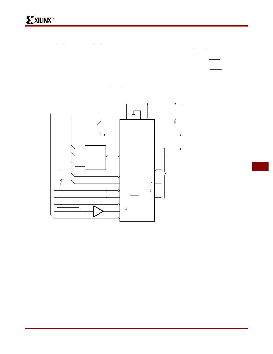
Peripheral Mode
Peripheral mode uses the trailing edge of the logic AND
condition of the CS0, CS1, CS2, and WS inputs to accept
byte-wide data from a microprocessor bus. In the lead
FPGA, this data is loaded into a double-buffered UART-like
parallel-to-serial converter and is serially shifted into the
internal logic. The lead FPGA presents the preamble data
(and all data that overflows the lead device) on the DOUT
pin.
The Ready/Busy output from the lead device acts as a
handshake signal to the microprocessor. RDY/BUSY goes
Low when a byte has been received, and goes High again
when the byte-wide input buffer has transferred its informa-
tion into the shift register, and the buffer is ready to receive
new data. The length of the BUSY signal depends on the
activity in the UART. If the shift register had been empty
when the new byte was received, the BUSY signal lasts for
only two CCLK periods. If the shift register was still full
when the new byte was received, the BUSY signal can be
as long as nine CCLK periods.
Note that after the last byte has been entered, only seven
of its bits are shifted out. CCLK remains High with DOUT
equal to bit 6 (the next-to-last bit) of the last byte entered.
X5991
ADDRESS
BUS
DATA
BUS
D0–7
ADDRESS
DECODE
LOGIC
CS0
...
RDY/BUSY
WS
RESET
...
OTHER
I/O PINS
D0–7
CCLK
DOUT
M2
HDC
LDC
FPGA
GENERAL-
PURPOSE
USER I/O
PINS
D/P
M0
M1 PWR
DWN
+5 V
CS2
CS1
CONTROL
SIGNALS
8
INIT
REPROGRAM
+5 V
5 k
*
IF READBACK IS
ACTIVATED, A
5-k
RESISTOR IS
REQUIRED IN SERIES
WITH M1
*
OPTIONAL
DAISY-CHAINED
FPGAs WITH DIFFERENT
CONFIGURATIONS
OC
Figure 27: Peripheral Mode Circuit Diagram
Product Obsolete or Under Obsolescence
相关PDF资料 |
PDF描述 |
|---|---|
| XC2S30-5PQ208I | IC FPGA 2.5V I-TEMP 208-PQFP |
| XC2S30-5PQ208C | IC FPGA 2.5V 216 CLB'S 208-PQFP |
| XC2S15-6CS144C | IC FPGA 2.5V C-TEMP 144-CSBGA |
| XC2S15-5CS144I | IC FPGA 2.5V I-TEMP 144-CSBGA |
| XC2S15-5CS144C | IC FPGA 2.5V C-TEMP 144-CSBGA |
相关代理商/技术参数 |
参数描述 |
|---|---|
| XC3030L-8VQ64I | 功能描述:IC FPGA I-TEMP 3.3V 64-VQFP RoHS:否 类别:集成电路 (IC) >> 嵌入式 - FPGA(现场可编程门阵列) 系列:XC3000A/L 产品变化通告:XC4000(E,L) Discontinuation 01/April/2002 标准包装:24 系列:XC4000E/X LAB/CLB数:100 逻辑元件/单元数:238 RAM 位总计:3200 输入/输出数:80 门数:3000 电源电压:4.5 V ~ 5.5 V 安装类型:表面贴装 工作温度:-40°C ~ 100°C 封装/外壳:120-BCBGA 供应商设备封装:120-CPGA(34.55x34.55) |
| XC3042 | 制造商:Xilinx 功能描述: |
| XC3042-100CB100B | 制造商:未知厂家 制造商全称:未知厂家 功能描述:Field Programmable Gate Array (FPGA) |
| XC3042-100CB100C | 制造商:未知厂家 制造商全称:未知厂家 功能描述:Field Programmable Gate Array (FPGA) |
| XC3042-100CB100M | 制造商:未知厂家 制造商全称:未知厂家 功能描述:Field Programmable Gate Array (FPGA) |
发布紧急采购,3分钟左右您将得到回复。