参数资料
| 型号: | XC3S250E-4FT256I |
| 厂商: | Xilinx Inc |
| 文件页数: | 176/227页 |
| 文件大小: | 0K |
| 描述: | IC FPGA SPARTAN 3E 256FTBGA |
| 标准包装: | 90 |
| 系列: | Spartan®-3E |
| LAB/CLB数: | 612 |
| 逻辑元件/单元数: | 5508 |
| RAM 位总计: | 221184 |
| 输入/输出数: | 172 |
| 门数: | 250000 |
| 电源电压: | 1.14 V ~ 1.26 V |
| 安装类型: | 表面贴装 |
| 工作温度: | -40°C ~ 100°C |
| 封装/外壳: | 256-LBGA |
| 供应商设备封装: | 256-FTBGA |
第1页第2页第3页第4页第5页第6页第7页第8页第9页第10页第11页第12页第13页第14页第15页第16页第17页第18页第19页第20页第21页第22页第23页第24页第25页第26页第27页第28页第29页第30页第31页第32页第33页第34页第35页第36页第37页第38页第39页第40页第41页第42页第43页第44页第45页第46页第47页第48页第49页第50页第51页第52页第53页第54页第55页第56页第57页第58页第59页第60页第61页第62页第63页第64页第65页第66页第67页第68页第69页第70页第71页第72页第73页第74页第75页第76页第77页第78页第79页第80页第81页第82页第83页第84页第85页第86页第87页第88页第89页第90页第91页第92页第93页第94页第95页第96页第97页第98页第99页第100页第101页第102页第103页第104页第105页第106页第107页第108页第109页第110页第111页第112页第113页第114页第115页第116页第117页第118页第119页第120页第121页第122页第123页第124页第125页第126页第127页第128页第129页第130页第131页第132页第133页第134页第135页第136页第137页第138页第139页第140页第141页第142页第143页第144页第145页第146页第147页第148页第149页第150页第151页第152页第153页第154页第155页第156页第157页第158页第159页第160页第161页第162页第163页第164页第165页第166页第167页第168页第169页第170页第171页第172页第173页第174页第175页当前第176页第177页第178页第179页第180页第181页第182页第183页第184页第185页第186页第187页第188页第189页第190页第191页第192页第193页第194页第195页第196页第197页第198页第199页第200页第201页第202页第203页第204页第205页第206页第207页第208页第209页第210页第211页第212页第213页第214页第215页第216页第217页第218页第219页第220页第221页第222页第223页第224页第225页第226页第227页
Spartan-3E FPGA Family: Functional Description
DS312 (v4.1) July 19, 2013
Product Specification
52
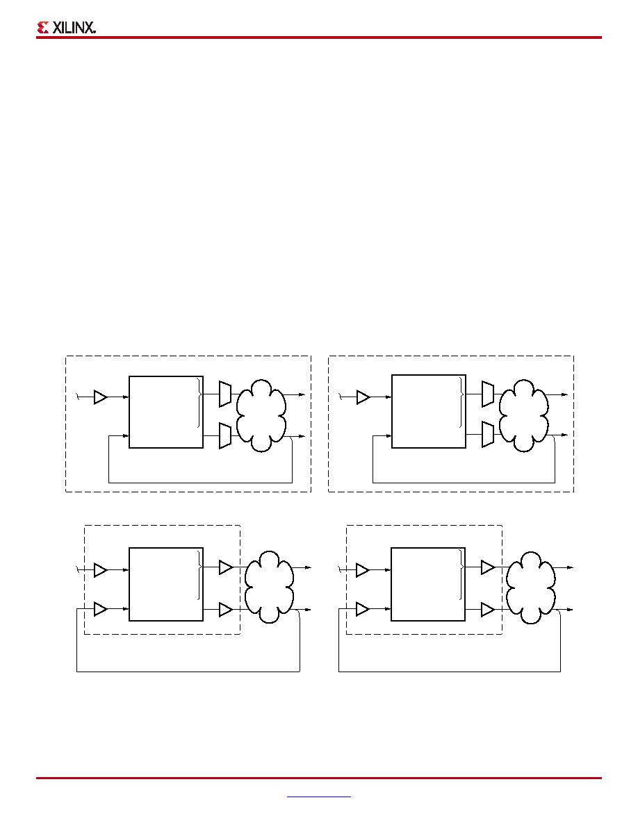
DLL Clock Output and Feedback Connections
As many as four of the nine DCM clock outputs can
simultaneously drive four of the BUFGMUX buffers on the
same die edge. All DCM clock outputs can simultaneously
drive general routing resources, including interconnect
leading to OBUF buffers.
The feedback loop is essential for DLL operation. Either the
CLK0 or CLK2X outputs feed back to the CLKFB input via a
BUFGMUX global buffer to eliminate the clock distribution
delay. The specific BUFGMUX buffer used to feed back the
CLK0 or CLK2X signal is ideally one of the BUFGMUX
buffers associated with a specific DCM, as shown in
The feedback path also phase-aligns the other seven DLL
outputs: CLK0, CLK90, CLK180, CLK270, CLKDV, CLK2X,
or CLK2X180. The CLK_FEEDBACK attribute value must
agree with the physical feedback connection. Use “1X” for
CLK0 feedback and “2X” for CLK2X feedback. If the DFS
unit is used stand-alone, without the DLL, then no feedback
is required and set the CLK_FEEDBACK attribute to
“NONE”.
Two basic cases determine how to connect the DLL clock
outputs and feedback connections: on-chip synchronization
and off-chip synchronization, which are illustrated in
Figure 42a through Figure 42d.
In the on-chip synchronization case in Figure 42a and
Figure 42b, it is possible to connect any of the DLL’s seven
output clock signals through general routing resources to
the FPGA’s internal registers. Either a Global Clock Buffer
(BUFG) or a BUFGMUX affords access to the global clock
network. As shown in Figure 42a, the feedback loop is
created by routing CLK0 (or CLK2X) in Figure 42b to a
global clock net, which in turn drives the CLKFB input.
In the off-chip synchronization case in Figure 42c and
Figure 42d, CLK0 (or CLK2X) plus any of the DLL’s other
output clock signals exit the FPGA using output buffers
(OBUF) to drive an external clock network plus registers on
the board. As shown in Figure 42c, the feedback loop is
formed by feeding CLK0 (or CLK2X) in Figure 42d back into
the FPGA, then to the DCM’s CLKFB input via a Global
Buffer Input, specified in Table 30.
X-Ref Target - Figure 42
Figure 42: Input Clock, Output Clock, and Feedback Connections for the DLL
DS099-2_09_082104
CLK90
CLK180
CLK270
CLKDV
CLK2X
CLK2X180
CLK0
Clock
Net Delay
BUFGMUX
BUFG
FPGA
(a) On-Chip with CLK0 Feedback
CLKIN
DCM
CLKFB
CLK90
CLK180
CLK270
CLKDV
CLK2X
CLK2X180
CLK0
Clock
Net Delay
IBUFG
FPGA
(c) Off-Chip with CLK0 Feedback
CLKIN
DCM
CLKFB
OBUF
CLK2X
IBUFG
FPGA
(d) Off-Chip with CLK2X Feedback
CLKIN
DCM
CLKFB
OBUF
CLK0
CLK90
CLK180
CLK270
CLKDV
CLK2X180
CLK2X
Clock
Net Delay
Clock
Net Delay
BUFGMUX
BUFG
FPGA
(b) On-Chip with CLK2X Feedback
CLKIN
DCM
CLKFB
CLK0
CLK90
CLK180
CLK270
CLKDV
CLK2X180
相关PDF资料 |
PDF描述 |
|---|---|
| 93LC76BT-I/ST | IC EEPROM 8KBIT 512X16 8-TSSOP |
| 93LC76BT-I/MS | IC EEPROM 8KBIT 512X16 8-MSOP |
| 93LC76B-I/ST | IC EEPROM 8KBIT 512X16 8-TSSOP |
| XC3S250E-5FTG256C | IC FPGA SPARTAN-3E 250K 256-FTBG |
| 93LC76B-I/MS | IC EEPROM 8KBIT 512X16 8-MSOP |
相关代理商/技术参数 |
参数描述 |
|---|---|
| XC3S250E-4FTG256C | 功能描述:IC SPARTAN-3E FPGA 250K 256-FTBG RoHS:是 类别:集成电路 (IC) >> 嵌入式 - FPGA(现场可编程门阵列) 系列:Spartan®-3E 标准包装:60 系列:XP LAB/CLB数:- 逻辑元件/单元数:10000 RAM 位总计:221184 输入/输出数:244 门数:- 电源电压:1.71 V ~ 3.465 V 安装类型:表面贴装 工作温度:0°C ~ 85°C 封装/外壳:388-BBGA 供应商设备封装:388-FPBGA(23x23) 其它名称:220-1241 |
| XC3S250E-4FTG256I | 功能描述:IC FPGA SPARTAN-3E 250K 256-FTBG RoHS:是 类别:集成电路 (IC) >> 嵌入式 - FPGA(现场可编程门阵列) 系列:Spartan®-3E 标准包装:40 系列:Spartan® 6 LX LAB/CLB数:3411 逻辑元件/单元数:43661 RAM 位总计:2138112 输入/输出数:358 门数:- 电源电压:1.14 V ~ 1.26 V 安装类型:表面贴装 工作温度:-40°C ~ 100°C 封装/外壳:676-BGA 供应商设备封装:676-FBGA(27x27) |
| XC3S250E-4PQ208C | 制造商:Xilinx 功能描述:FPGA SPARTAN-3E 250K GATES 5508 CELLS 572MHZ 90NM 1.2V 208PQ - Trays |
| XC3S250E-4PQ208CES | 制造商:Xilinx 功能描述: |
| XC3S250E-4PQ208I | 功能描述:IC FPGA SPARTAN 3E 208PQFP RoHS:否 类别:集成电路 (IC) >> 嵌入式 - FPGA(现场可编程门阵列) 系列:Spartan®-3E 标准包装:40 系列:Spartan® 6 LX LAB/CLB数:3411 逻辑元件/单元数:43661 RAM 位总计:2138112 输入/输出数:358 门数:- 电源电压:1.14 V ~ 1.26 V 安装类型:表面贴装 工作温度:-40°C ~ 100°C 封装/外壳:676-BGA 供应商设备封装:676-FBGA(27x27) |
发布紧急采购,3分钟左右您将得到回复。