参数资料
| 型号: | XC4008E-4PG191I |
| 厂商: | Xilinx Inc |
| 文件页数: | 57/68页 |
| 文件大小: | 0K |
| 描述: | IC FPGA I-TEMP 5V 4SPD 191-CPGA |
| 产品变化通告: | XC4000(E,L) Discontinuation 01/April/2002 |
| 标准包装: | 12 |
| 系列: | XC4000E/X |
| LAB/CLB数: | 324 |
| 逻辑元件/单元数: | 770 |
| RAM 位总计: | 10368 |
| 输入/输出数: | 144 |
| 门数: | 8000 |
| 电源电压: | 4.5 V ~ 5.5 V |
| 安装类型: | 表面贴装 |
| 工作温度: | -40°C ~ 100°C |
| 封装/外壳: | 191-BCBGA |
| 供应商设备封装: | 191-CPGA(47.25x47.25) |
第1页第2页第3页第4页第5页第6页第7页第8页第9页第10页第11页第12页第13页第14页第15页第16页第17页第18页第19页第20页第21页第22页第23页第24页第25页第26页第27页第28页第29页第30页第31页第32页第33页第34页第35页第36页第37页第38页第39页第40页第41页第42页第43页第44页第45页第46页第47页第48页第49页第50页第51页第52页第53页第54页第55页第56页当前第57页第58页第59页第60页第61页第62页第63页第64页第65页第66页第67页第68页
R
XC4000E and XC4000X Series Field Programmable Gate Arrays
6-64
May 14, 1999 (Version 1.6)
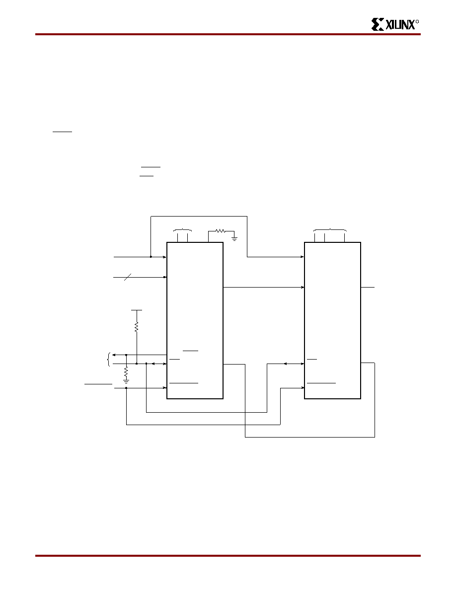
Synchronous Peripheral Mode
Synchronous Peripheral mode can also be considered
Slave Parallel mode. An external signal drives the CCLK
input(s) of the FPGA(s). The rst byte of parallel congura-
tion data must be available at the Data inputs of the lead
FPGA a short setup time before the rising CCLK edge.
Subsequent data bytes are clocked in on every eighth con-
secutive rising CCLK edge.
The same CCLK edge that accepts data, also causes the
RDY/BUSY output to go High for one CCLK period. The pin
name is a misnomer. In Synchronous Peripheral mode it is
really an ACKNOWLEDGE signal. Synchronous operation
does not require this response, but it is a meaningful signal
for test purposes. Note that RDY/BUSY is pulled High with
a high-impedance pullup prior to INIT going High.
The lead FPGA serializes the data and presents the pre-
amble data (and all data that overows the lead device) on
its DOUT pin. There is an internal delay of 1.5 CCLK peri-
ods, which means that DOUT changes on the falling CCLK
edge, and the next FPGA in the daisy chain accepts data
on the subsequent rising CCLK edge.
In order to complete the serial shift operation, 10 additional
CCLK rising edges are required after the last data byte has
been loaded, plus one more CCLK cycle for each
daisy-chained device.
Synchronous Peripheral mode is selected by a <011> on
the mode pins (M2, M1, M0).
X9027
CONTROL
SIGNALS
DATA BUS
PROGRAM
DOUT
M0 M1
M2
D0-7
INIT
DONE
PROGRAM
4.7 k
4.7 k
4.7 k
RDY/BUSY
VCC
OPTIONAL
DAISY-CHAINED
FPGAs
NOTE:
M2 can be shorted to Ground
if not used as I/O
CCLK
CLOCK
PROGRAM
DOUT
XC4000E/X
SLAVE
XC4000E/X
SYNCHRO-
NOUS
PERIPHERAL
M0 M1
N/C
8
M2
DIN
INIT
DONE
CCLK
N/C
Figure 56: Synchronous Peripheral Mode Circuit Diagram
Product Obsolete or Under Obsolescence
相关PDF资料 |
PDF描述 |
|---|---|
| XC4008E-4PG191C | IC FPGA C-TEMP 5V 4SPD 191-CPGA |
| XC4008E-4PC84I | IC FPGA I-TEMP 5V 4SPD 84-PLCC |
| 1-487378-1 | CONN RECEPT 12POS .100 SLIMLINE |
| ACB110DHFT | CONN EDGECARD 220POS .050 SMD |
| 487526-8 | CONN RCPT 9POS.100 SLIM W/LATCH |
相关代理商/技术参数 |
参数描述 |
|---|---|
| XC4008E-4PG191M | 制造商:未知厂家 制造商全称:未知厂家 功能描述:Field Programmable Gate Array (FPGA) |
| XC4008E-4PQ160C | 功能描述:IC FPGA 324 CLB'S 160-PQFP RoHS:否 类别:集成电路 (IC) >> 嵌入式 - FPGA(现场可编程门阵列) 系列:XC4000E/X 产品变化通告:XC4000(E,L) Discontinuation 01/April/2002 标准包装:24 系列:XC4000E/X LAB/CLB数:100 逻辑元件/单元数:238 RAM 位总计:3200 输入/输出数:80 门数:3000 电源电压:4.5 V ~ 5.5 V 安装类型:表面贴装 工作温度:-40°C ~ 100°C 封装/外壳:120-BCBGA 供应商设备封装:120-CPGA(34.55x34.55) |
| XC4008E-4PQ160I | 功能描述:IC FPGA I-TEMP 5V 4SPD 160-PQFP RoHS:否 类别:集成电路 (IC) >> 嵌入式 - FPGA(现场可编程门阵列) 系列:XC4000E/X 标准包装:1 系列:Kintex-7 LAB/CLB数:25475 逻辑元件/单元数:326080 RAM 位总计:16404480 输入/输出数:350 门数:- 电源电压:0.97 V ~ 1.03 V 安装类型:表面贴装 工作温度:0°C ~ 85°C 封装/外壳:900-BBGA,FCBGA 供应商设备封装:900-FCBGA(31x31) 其它名称:122-1789 |
| XC4008E-4PQ208C | 功能描述:IC FPGA 324 CLB'S 208-PQFP RoHS:否 类别:集成电路 (IC) >> 嵌入式 - FPGA(现场可编程门阵列) 系列:XC4000E/X 产品变化通告:XC4000(E,L) Discontinuation 01/April/2002 标准包装:24 系列:XC4000E/X LAB/CLB数:100 逻辑元件/单元数:238 RAM 位总计:3200 输入/输出数:80 门数:3000 电源电压:4.5 V ~ 5.5 V 安装类型:表面贴装 工作温度:-40°C ~ 100°C 封装/外壳:120-BCBGA 供应商设备封装:120-CPGA(34.55x34.55) |
| XC4008E-4PQ208C0262 | 制造商:Xilinx 功能描述: |
发布紧急采购,3分钟左右您将得到回复。