- 您现在的位置:买卖IC网 > PDF目录245729 > XC4013E-3PQ240C (XILINX INC) XC4000E and XC4000X Series Field Programmable Gate Arrays PDF资料下载
参数资料
| 型号: | XC4013E-3PQ240C |
| 厂商: | XILINX INC |
| 元件分类: | FPGA |
| 英文描述: | XC4000E and XC4000X Series Field Programmable Gate Arrays |
| 中文描述: | FPGA, 576 CLBS, 10000 GATES, 125 MHz, PQFP240 |
| 文件页数: | 16/17页 |
| 文件大小: | 75K |
| 代理商: | XC4013E-3PQ240C |
R
XC4000E and XC4000X Series Field Programmable Gate Arrays
6-108
February 11, 2000 (Version 1.8)
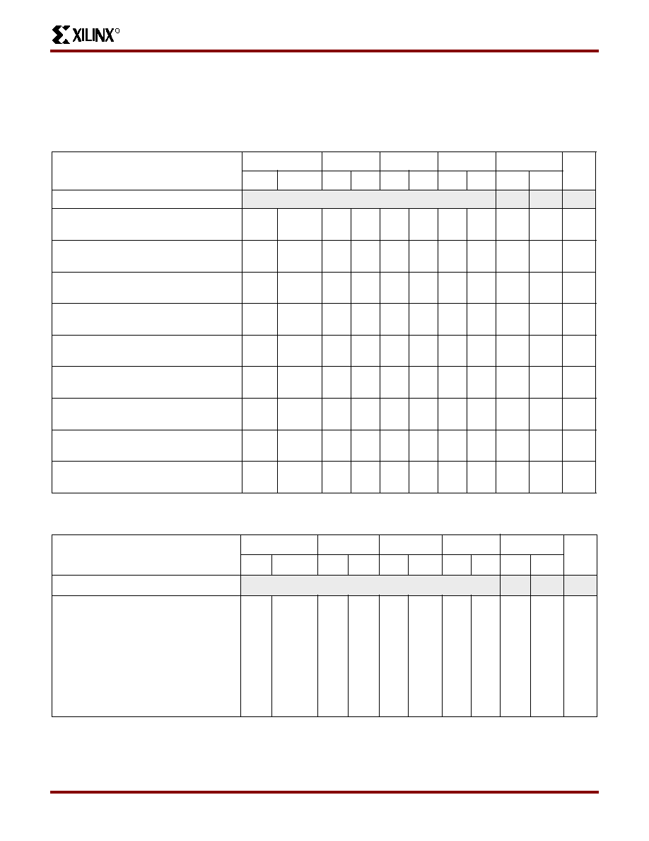
CLB Edge-Triggered (Synchronous) RAM Switching Characteristic Guidelines
Testing of switching parameters is modeled after testing methods specied by MIL-M-38510/605. All devices are 100% functionally tested.
Internal timing parameters are derived from measuring internal test patterns. Listed below are representative values. For more specic, more
precise, and worst-case guaranteed data, use the values reported by the static timing analyzer (TRCE in the Xilinx Development System) and
back-annotated to the simulation net list. All timing parameters assume worst-case operating conditions (supply voltage and junction
temperature). Values apply to all XC4000E devices unless otherwise noted.
Single Port RAM
Speed Grade
-4
-3
-2
-1
Units
Size
Symbol
Min
Max
Min
Max
Min
Max
Min
Max
Write Operation
Address write cycle time (clock K period)
16x2
32x1
TWCS
TWCTS
15.0
14.4
11.6
8.0
ns
Clock K pulse width (active edge)
16x2
32x1
TWPS
TWPTS
7.5
1ms
7.2
1ms
5.8
1ms
4.0
ns
Address setup time before clock K
16x2
32x1
TASS
TASTS
2.8
2.4
2.0
1.5
ns
Address hold time after clock K
16x2
32x1
TAHS
TAHTS
0
ns
DIN setup time before clock K
16x2
32x1
TDSS
TDSTS
3.5
2.5
3.2
1.9
2.7
1.7
1.5
ns
DIN hold time after clock K
16x2
32x1
TDHS
TDHTS
0
ns
WE setup time before clock K
16x2
32x1
TWSS
TWSTS
2.2
2.0
1.6
1.5
ns
WE hold time after clock K
16x2
32x1
TWHS
TWHTS
0
ns
Data valid after clock K
16x2
32x1
TWOS
TWOTS
10.3
11.6
8.8
10.3
7.9
9.3
6.5
7.0
ns
Note 1: Timing for the 16x1 RAM option is identical to 16x2 RAM timing.
Note 2: Applicable Read timing specications are identical to Level-Sensitive Read timing.
Dual-Port RAM
Speed Grade
-4
-3
-2
-1
Units
Size
Symbol
Min
Max
Min
Max
Min
Max
Min
Max
Write Operation
Address write cycle time (clock K period)
Clock K pulse width (active edge)
Address setup time before clock K
Address hold time after clock K
DIN setup time before clock K
DIN hold time after clock K
WE setup time before clock K
WE hold time after clock K
Data valid after clock K
16x1
TWCDS
TWPDS
TASDS
TAHDS
TDSDS
TDHDS
TWSDS
TWHDS
TWODS
15.0
7.5
2.8
0
2.2
0
2.2
0.3
1 ms
10.0
14.4
7.2
2.5
0
2.5
0
1.8
0
1 ms
7.8
11.6
5.8
2.1
0
1.6
0
1.6
0
1ms
7.0
8.0
4.0
1.5
0
1.5
0
1.5
0
6.5
ns
Note: Applicable Read timing specications are identical to Level-Sensitive Read timing
相关PDF资料 |
PDF描述 |
|---|---|
| XC4013E-3PQ240I | XC4000E and XC4000X Series Field Programmable Gate Arrays |
| XC4003E-4PC84I | XC4000E and XC4000X Series Field Programmable Gate Arrays |
| XC4008E-4PQ208I | High Insulation Power Relay (Sealed 1 Form C 1-Coil Latch) |
| ZW-10-08-S-D-200 | 20 CONTACT(S), MALE, STRAIGHT BOARD STACKING CONNECTOR, SOLDER |
| ZW-10-08-S-T-200 | 30 CONTACT(S), MALE, STRAIGHT BOARD STACKING CONNECTOR, SOLDER |
相关代理商/技术参数 |
参数描述 |
|---|---|
| XC4013E-3PQ240C0119 | 制造商:Xilinx 功能描述: |
| XC4013E-3PQ240I | 功能描述:IC FPGA I-TEMP 5V 3SPD 240-PQFP RoHS:否 类别:集成电路 (IC) >> 嵌入式 - FPGA(现场可编程门阵列) 系列:XC4000E/X 标准包装:1 系列:Kintex-7 LAB/CLB数:25475 逻辑元件/单元数:326080 RAM 位总计:16404480 输入/输出数:350 门数:- 电源电压:0.97 V ~ 1.03 V 安装类型:表面贴装 工作温度:0°C ~ 85°C 封装/外壳:900-BBGA,FCBGA 供应商设备封装:900-FCBGA(31x31) 其它名称:122-1789 |
| XC4013E-3PQ240M | 制造商:XILINX 制造商全称:XILINX 功能描述:XC4000E and XC4000X Series Field Programmable Gate Arrays |
| XC4013E-3TQ240C | 制造商:XILINX 制造商全称:XILINX 功能描述:XC4000E and XC4000X Series Field Programmable Gate Arrays |
| XC4013E-3TQ240I | 制造商:XILINX 制造商全称:XILINX 功能描述:XC4000E and XC4000X Series Field Programmable Gate Arrays |
发布紧急采购,3分钟左右您将得到回复。