- 您现在的位置:买卖IC网 > PDF目录245729 > XC4013E-3PQ240C (XILINX INC) XC4000E and XC4000X Series Field Programmable Gate Arrays PDF资料下载
参数资料
| 型号: | XC4013E-3PQ240C |
| 厂商: | XILINX INC |
| 元件分类: | FPGA |
| 英文描述: | XC4000E and XC4000X Series Field Programmable Gate Arrays |
| 中文描述: | FPGA, 576 CLBS, 10000 GATES, 125 MHz, PQFP240 |
| 文件页数: | 5/17页 |
| 文件大小: | 75K |
| 代理商: | XC4013E-3PQ240C |
R
February 11, 2000 (Version 1.8)
6-113
XC4000E and XC4000X Series Field Programmable Gate Arrays
6
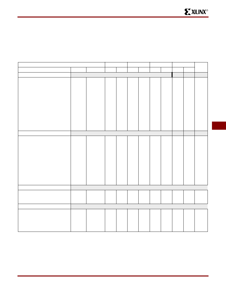
XC4000E IOB Input Switching Characteristic Guidelines
Testing of switching parameters is modeled after testing methods specied by MIL-M-38510/605. All devices are 100%
functionally tested. Pin-to-pin timing parameters are derived from measuring external and internal test patterns and are
guaranteed over worst-case operating conditions (supply voltage and junction temperature). Listed below are representative
values for typical pin locations and normal clock loading. For more specic, more precise, and worst-case guaranteed data,
reecting the actual routing structure, use the values provided by the static timing analyzer (TRCE in the Xilinx Development
System) and back-annotated to the simulation net list. These path delays, provided as a guideline, have been extracted from
the static timing analyzer report. Values apply to all XC4000E devices unless otherwise noted.
Speed Grade
-4
-3
-2
-1
Units
Description
Symbol
Device
Min
Max
Min
Max
Min
Max
Min
Max
Propagation Delays (TTL Inputs)
Pad to I1, I2
Pad to I1, I2 via transparent
latch, no delay
with delay
TPID
TPLI
TPDLI
All devices
XC4003E
XC4005E
XC4006E
XC4008E
XC4010E
XC4013E
XC4020E
XC4025E
3.0
4.8
10.4
10.8
11.0
11.4
13.8
2.5
3.6
9.3
9.6
10.2
10.6
10.8
11.2
12.4
13.7
2.0
3.6
6.9
7.4
8.1
8.2
8.3
9.8
11.5
12.4
1.4
2.8
6.4
6.5
6.9
7.0
7.3
8.4
9.0
–
ns
Propagation Delays (CMOS Inputs)
Pad to I1, I2
Pad to I1, I2 via transparent
latch, no delay
with delay
TPIDC
TPLIC
TPDLIC
All devices
XC4003E
XC4005E
XC4006E
XC4008E
XC4010E
XC4013E
XC4020E
XC4025E
5.5
8.8
16.5
16.8
17.3
17.5
18.0
20.8
4.1
6.8
12.4
13.2
13.4
13.8
14.0
14.4
15.6
3.7
6.2
11.0
11.9
12.1
12.4
12.6
13.0
14.0
1.9
3.3
6.9
7.0
7.4
7.8
9.0
9.5
–
ns
Propagation Delays
Clock (IK) to I1, I2 (flip-flop)
Clock (IK) to I1, I2
(latch enable, active Low)
TIKRI
TIKLI
All devices
5.6
6.2
2.8
4.0
2.8
3.9
2.7
3.2
ns
Hold Times (Note 1)
Pad to Clock (IK), no delay
with delay
Clock Enable (EC) to Clock (IK),
no delay
with delay
TIKPI
TIKPID
TIKEC
TIKECD
All devices
0
1.5
0
1.5
0
0.9
0
ns
Note 1: Input pad setup and hold times are specied with respect to the internal clock (IK). For setup and hold times with respect to the
clock input pin, see the pin-to-pin parameters in the Guaranteed Input and Output Parameters table.
Note 2: Voltage levels of unused pads, bonded or unbonded, must be valid logic levels. Each can be congured with the internal pull-up
(default) or pull-down resistor, or congured as a driven output, or can be driven from an external source.
相关PDF资料 |
PDF描述 |
|---|---|
| XC4013E-3PQ240I | XC4000E and XC4000X Series Field Programmable Gate Arrays |
| XC4003E-4PC84I | XC4000E and XC4000X Series Field Programmable Gate Arrays |
| XC4008E-4PQ208I | High Insulation Power Relay (Sealed 1 Form C 1-Coil Latch) |
| ZW-10-08-S-D-200 | 20 CONTACT(S), MALE, STRAIGHT BOARD STACKING CONNECTOR, SOLDER |
| ZW-10-08-S-T-200 | 30 CONTACT(S), MALE, STRAIGHT BOARD STACKING CONNECTOR, SOLDER |
相关代理商/技术参数 |
参数描述 |
|---|---|
| XC4013E-3PQ240C0119 | 制造商:Xilinx 功能描述: |
| XC4013E-3PQ240I | 功能描述:IC FPGA I-TEMP 5V 3SPD 240-PQFP RoHS:否 类别:集成电路 (IC) >> 嵌入式 - FPGA(现场可编程门阵列) 系列:XC4000E/X 标准包装:1 系列:Kintex-7 LAB/CLB数:25475 逻辑元件/单元数:326080 RAM 位总计:16404480 输入/输出数:350 门数:- 电源电压:0.97 V ~ 1.03 V 安装类型:表面贴装 工作温度:0°C ~ 85°C 封装/外壳:900-BBGA,FCBGA 供应商设备封装:900-FCBGA(31x31) 其它名称:122-1789 |
| XC4013E-3PQ240M | 制造商:XILINX 制造商全称:XILINX 功能描述:XC4000E and XC4000X Series Field Programmable Gate Arrays |
| XC4013E-3TQ240C | 制造商:XILINX 制造商全称:XILINX 功能描述:XC4000E and XC4000X Series Field Programmable Gate Arrays |
| XC4013E-3TQ240I | 制造商:XILINX 制造商全称:XILINX 功能描述:XC4000E and XC4000X Series Field Programmable Gate Arrays |
发布紧急采购,3分钟左右您将得到回复。