- 您现在的位置:买卖IC网 > PDF目录300146 > XC4013XL-3BG256I (XILINX INC) XC4000E and XC4000X Series Field Programmable Gate Arrays PDF资料下载
参数资料
| 型号: | XC4013XL-3BG256I |
| 厂商: | XILINX INC |
| 元件分类: | FPGA |
| 英文描述: | XC4000E and XC4000X Series Field Programmable Gate Arrays |
| 中文描述: | FPGA, 576 CLBS, 10000 GATES, 166 MHz, PBGA256 |
| 文件页数: | 6/16页 |
| 文件大小: | 69K |
| 代理商: | XC4013XL-3BG256I |
R
XC4000E and XC4000X Series Field Programmable Gate Arrays
6-86
DS005 (v. 1.8 October 18, 1999 - Product Specication
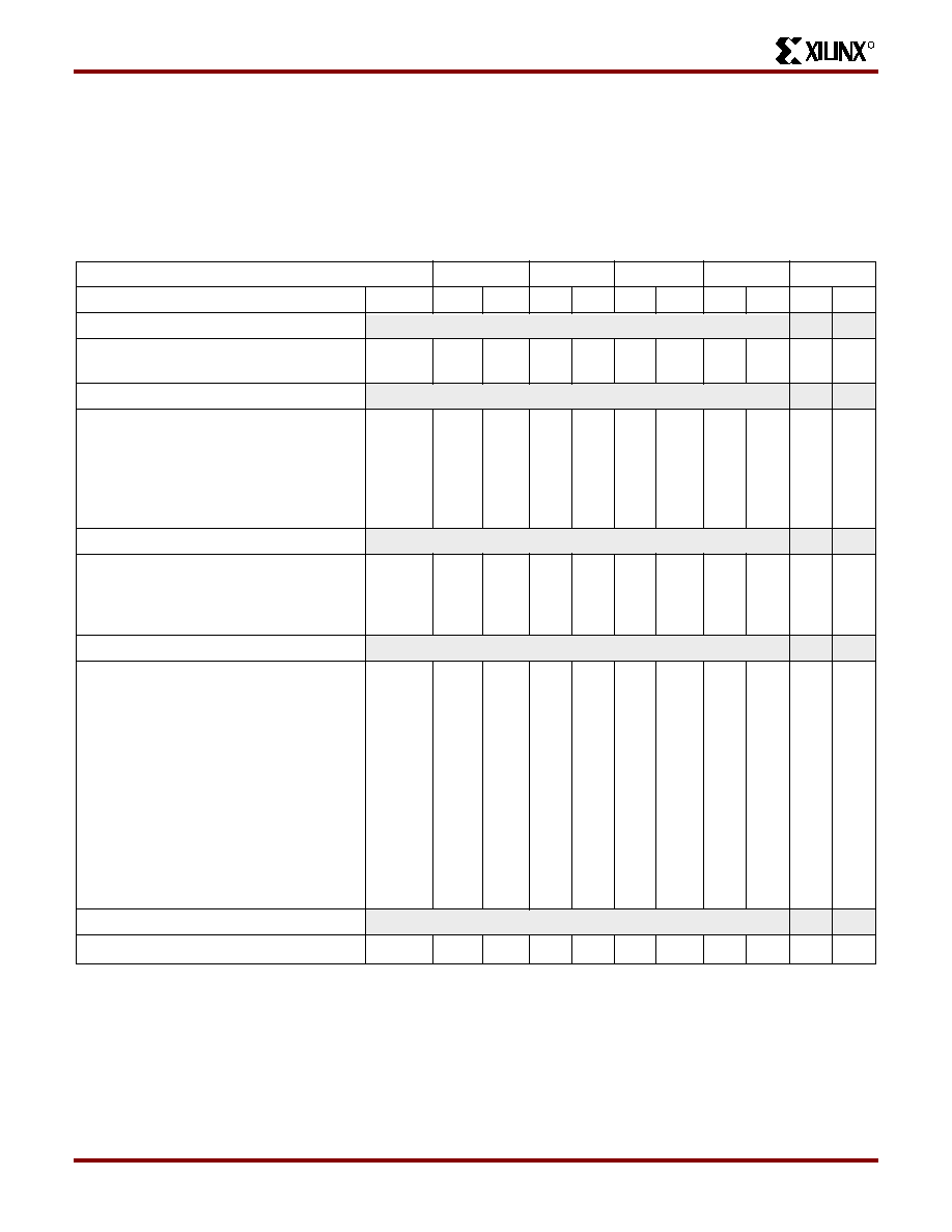
XC4000XL IOB Output Switching Characteristic Guidelines
Testing of switching parameters is modeled after testing methods specied by MIL-M-38510/605. All devices are 100%
functionally tested. Internal timing parameters are derived from measuring internal test patterns. Listed below are
representative values. For more specic, more precise, and worst-case guaranteed data, use the values reported by the
static timing analyzer (TRCE in the Xilinx Development System) and back-annotated to the simulation netlist. These path
delays, provided as a guideline, have been extracted from the static timing analyzer report. All timing parameters assume
worst-case operating conditions (supply voltage and junction temperature). For Propagation Delays, slew-rate = fast unless
otherwise noted. Values are expressed in nanoseconds unless otherwise noted.
-3
-2
-1
-09
-08
Description
Symbol
Min
Max
Min
Max
Min
Max
Min
Max
Min
Max
Clocks
Clock High
Clock Low
TCH
TCL
3.0
2.8
2.5
2.3
2.1
Propagation Delays
Clock (OK) to Pad
Output (O) to Pad
3-state to Pad hi-Z (slew-rate independent)
3-state to Pad active and valid
Output (O) to Pad via Fast Output MUX
Select (OK) to Pad via Fast MUX
TOKPOF
TOPF
TTSHZ
TTSONF
TOFPF
TOKFPF
5.0
4.1
4.0
4.4
5.5
5.1
4.3
3.6
3.5
3.8
4.8
4.5
3.8
3.1
3.0
3.3
4.2
3.9
3.5
3.0
2.9
3.3
4.0
3.7
3.3
2.8
2.9
3.3
3.7
3.4
Setup and Hold Times
Output (O) to clock (OK) setup time
Output (O) to clock (OK) hold time
Clock Enable (EC) to clock (OK) setup time
Clock Enable (EC) to clock (OK) hold time
TOOK
TOKO
TECOK
TOKEC
0.5
0.0
0.3
0.4
0.0
0.2
0.3
0.0
0.1
0.3
0.0
0.3
0.0
Global Set/Reset
Minimum GSR pulse width
Delay from GSR input to any Pad
XC4002XL
XC4005XL
XC4010XL
XC4013XL
XC4020XL
XC4028XL
XC4036XL
XC4044XL
XC4052XL
XC4062XL
XC4085XL
TMRW
TRPO*
19.8
14.3
15.9
18.5
20.5
23.2
25.1
27.1
29.7
31.7
33.7
39.0
17.3
12.5
13.8
16.1
17.8
20.1
21.9
23.6
25.9
27.6
29.3
33.9
15.0
10.9
12.0
14.0
15.5
17.5
19.0
20.5
22.5
24.0
25.5
29.5
14.0
10.3
11.4
13.3
14.7
16.6
17.6
19.4
21.4
22.8
24.2
28.0
14.0
19.3
23.5
Slew Rate Adjustment
For output SLOW option add
TSLOW
3.0
2.5
2.0
1.7
1.6
Note: Output timing is measured at ~50% VCC threshold, with 50 pF external capacitive loads.
* Indicates Minimum Amount of Time to Assure Valid Data.
相关PDF资料 |
PDF描述 |
|---|---|
| XC4013XL-3PQ160C | XC4000E and XC4000X Series Field Programmable Gate Arrays |
| XC4013XL-3PQ160I | XC4000E and XC4000X Series Field Programmable Gate Arrays |
| XC4013XL-3PQ208C | XC4000E and XC4000X Series Field Programmable Gate Arrays |
| XC4013XL-3PQ208I | XC4000E and XC4000X Series Field Programmable Gate Arrays |
| XC4013XL-3PQ240C | XC4000E and XC4000X Series Field Programmable Gate Arrays |
相关代理商/技术参数 |
参数描述 |
|---|---|
| XC4013XL-3BG256M | 制造商:XILINX 制造商全称:XILINX 功能描述:XC4000E and XC4000X Series Field Programmable Gate Arrays |
| XC4013XL-3HT144C | 功能描述:IC FPGA C-TEMP 3.3V 3SPD 144HQFP RoHS:否 类别:集成电路 (IC) >> 嵌入式 - FPGA(现场可编程门阵列) 系列:XC4000E/X 标准包装:1 系列:Kintex-7 LAB/CLB数:25475 逻辑元件/单元数:326080 RAM 位总计:16404480 输入/输出数:350 门数:- 电源电压:0.97 V ~ 1.03 V 安装类型:表面贴装 工作温度:0°C ~ 85°C 封装/外壳:900-BBGA,FCBGA 供应商设备封装:900-FCBGA(31x31) 其它名称:122-1789 |
| XC4013XL-3HT144I | 功能描述:IC FPGA I-TEMP 3.3V 3SPD 144HQFP RoHS:否 类别:集成电路 (IC) >> 嵌入式 - FPGA(现场可编程门阵列) 系列:XC4000E/X 标准包装:1 系列:Kintex-7 LAB/CLB数:25475 逻辑元件/单元数:326080 RAM 位总计:16404480 输入/输出数:350 门数:- 电源电压:0.97 V ~ 1.03 V 安装类型:表面贴装 工作温度:0°C ~ 85°C 封装/外壳:900-BBGA,FCBGA 供应商设备封装:900-FCBGA(31x31) 其它名称:122-1789 |
| XC4013XL-3HT144M | 制造商:XILINX 制造商全称:XILINX 功能描述:XC4000E and XC4000X Series Field Programmable Gate Arrays |
| XC4013XL-3HT176C | 功能描述:IC FPGA C 3.3V 3SPD 176HTQFP RoHS:否 类别:集成电路 (IC) >> 嵌入式 - FPGA(现场可编程门阵列) 系列:XC4000E/X 标准包装:1 系列:Kintex-7 LAB/CLB数:25475 逻辑元件/单元数:326080 RAM 位总计:16404480 输入/输出数:350 门数:- 电源电压:0.97 V ~ 1.03 V 安装类型:表面贴装 工作温度:0°C ~ 85°C 封装/外壳:900-BBGA,FCBGA 供应商设备封装:900-FCBGA(31x31) 其它名称:122-1789 |
发布紧急采购,3分钟左右您将得到回复。