参数资料
| 型号: | XC4VLX100-10FFG1148C |
| 厂商: | Xilinx Inc |
| 文件页数: | 47/58页 |
| 文件大小: | 0K |
| 描述: | IC FPGA VIRTEX-4 100K 1148-FBGA |
| 标准包装: | 1 |
| 系列: | Virtex®-4 LX |
| LAB/CLB数: | 12288 |
| 逻辑元件/单元数: | 110592 |
| RAM 位总计: | 4423680 |
| 输入/输出数: | 768 |
| 电源电压: | 1.14 V ~ 1.26 V |
| 安装类型: | 表面贴装 |
| 工作温度: | 0°C ~ 85°C |
| 封装/外壳: | 1148-BBGA,FCBGA |
| 供应商设备封装: | 1148-FCPBGA(35x35) |
| 其它名称: | 122-1486 |
第1页第2页第3页第4页第5页第6页第7页第8页第9页第10页第11页第12页第13页第14页第15页第16页第17页第18页第19页第20页第21页第22页第23页第24页第25页第26页第27页第28页第29页第30页第31页第32页第33页第34页第35页第36页第37页第38页第39页第40页第41页第42页第43页第44页第45页第46页当前第47页第48页第49页第50页第51页第52页第53页第54页第55页第56页第57页第58页
Virtex-4 FPGA Data Sheet: DC and Switching Characteristics
DS302 (v3.7) September 9, 2009
Product Specification
51
Production Stepping
The Virtex-4 FPGA stepping identification system denotes
the capability improvement of production released devices.
By definition, devices from one stepping are functional
supersets of previous devices. Bitstreams compiled for a
device with an earlier stepping are guaranteed to operate
correctly in subsequent device steppings.
New device steppings can be shipped in place of earlier
device steppings. Existing production designs are guaran-
teed on new device steppings. To take advantage of the
capabilities of a newer device stepping, customers are able
to order a new stepping version and compile a new bit-
stream.
Production devices are marked with a stepping version, with
the exception of some step 1 devices. Designs should be
compiled with a CONFIG STEPPING parameter set to a
specific stepping version. This parameter is set in the UCF
file:
CONFIG STEPPING = “#”; (where # is the stepping
version)
The default stepping level used by the ISE software is
reported in the PAR report.
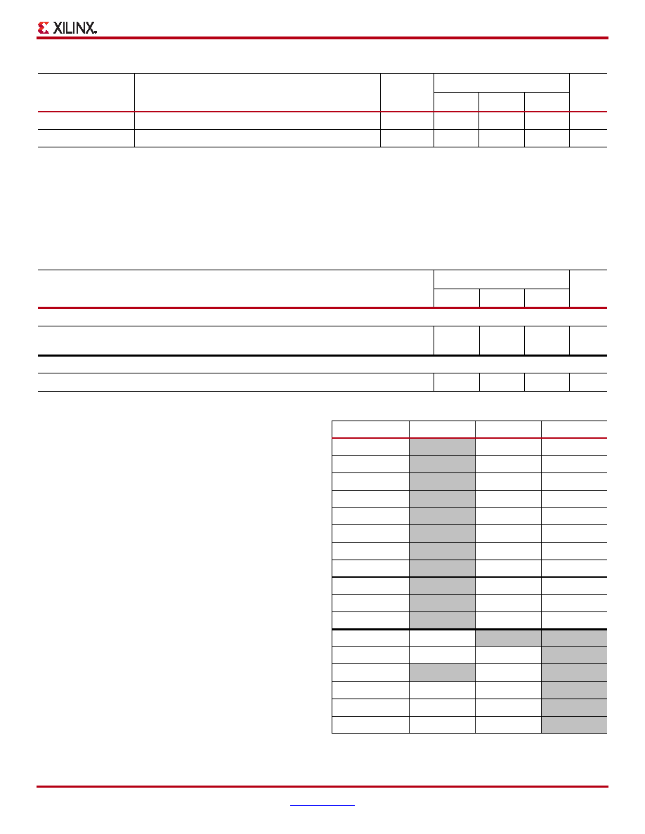
Table 63 shows the JTAG ID code by step.
Table 61: Sample Window
Symbol
Description
Device
Speed Grade
Units
-12
-11
-10
TSAMP
Sampling Error at Receiver Pins(1)
All
450
500
550
ps
TSAMP_BUFIO
Sampling Error at Receiver Pins using BUFIO(2)
All
350
400
450
ps
Notes:
1.
This parameter indicates the total sampling error of Virtex-4 FPGA DDR input registers across voltage, temperature, and process. The
characterization methodology uses the DCM to capture the DDR input registers’ edges of operation. These measurements include:
- CLK0 DCM jitter
- DCM accuracy (phase offset)
- DCM phase shift resolution
These measurements do not include package or clock tree skew.
2.
This parameter indicates the total sampling error of Virtex-4 FPGA DDR input registers across voltage, temperature, and process. The
characterization methodology uses the BUFIO clock network and IDELAY to capture the DDR input registers’ edges of operation. These
measurements do not include package or clock tree skew.
Table 62: ChipSync Pin-to-Pin Setup/Hold and Clock-to-Out
Symbol
Description
Speed Grade
Units
-12
-11
-10
Data Input Setup and Hold Times Relative to a Forwarded Clock Input Pin Using BUFIO
TPSCS /TPHCS
Setup/Hold of I/O clock across multiple clock regions
–0.45
0.97
–0.45
1.08
–0.44
1.17
ns
Pin-to-Pin Clock-to-Out Using BUFIO
TICKOFCS
Clock-to-Out of I/O clock across multiple clock regions
4.10
4.54
5.02
ns
Table 63: JTAG ID Code by Step
Device
Step 0
Step 1
Step 2
XC4VLX15
35
XC4VLX25
9A
XC4VLX40
35
XC4VLX60
2 or 3
4 or 5
XC4VLX80
35
XC4VLX100
2 or 3
4 or 5
XC4VLX160
0 or 3
4 or 5
XC4VLX200
0 or 3
2 or 5
XC4VSX25
24
XC4VSX35
24
XC4VSX55
24
XC4VFX12
0 or 2
XC4VFX20
26
XC4VFX40
0
XC4VFX60
28
XC4VFX100
06
XC4VFX140
04
Notes:
1.
Shaded cells represent devices not produced at that stepping.
相关PDF资料 |
PDF描述 |
|---|---|
| W25X40CLZPIG | IC FLASH SPI 4MBIT 8WSON |
| W25X40CLSNIG | IC FLASH SPI 4MBIT 8SOIC |
| IDT71256SA15PZG8 | IC SRAM 256KBIT 15NS 28TSOP |
| AMM36DRKH-S13 | CONN EDGECARD 72POS .156 EXTEND |
| ABB60DHAS-S621 | CONN EDGECARD 120PS R/A .050 SLD |
相关代理商/技术参数 |
参数描述 |
|---|---|
| XC4VLX100-10FFG1148I | 功能描述:IC FPGA VIRTEX-4LX 100K 1148FBGA RoHS:是 类别:集成电路 (IC) >> 嵌入式 - FPGA(现场可编程门阵列) 系列:Virtex®-4 LX 产品变化通告:XC4000(E,L) Discontinuation 01/April/2002 标准包装:24 系列:XC4000E/X LAB/CLB数:100 逻辑元件/单元数:238 RAM 位总计:3200 输入/输出数:80 门数:3000 电源电压:4.5 V ~ 5.5 V 安装类型:表面贴装 工作温度:-40°C ~ 100°C 封装/外壳:120-BCBGA 供应商设备封装:120-CPGA(34.55x34.55) |
| XC4VLX100-10FFG1513C | 功能描述:IC FPGA VIRTEX-4 100K 1513-FBGA RoHS:是 类别:集成电路 (IC) >> 嵌入式 - FPGA(现场可编程门阵列) 系列:Virtex®-4 LX 产品变化通告:XC4000(E,L) Discontinuation 01/April/2002 标准包装:24 系列:XC4000E/X LAB/CLB数:100 逻辑元件/单元数:238 RAM 位总计:3200 输入/输出数:80 门数:3000 电源电压:4.5 V ~ 5.5 V 安装类型:表面贴装 工作温度:-40°C ~ 100°C 封装/外壳:120-BCBGA 供应商设备封装:120-CPGA(34.55x34.55) |
| XC4VLX100-10FFG1513I | 功能描述:IC FPGA VIRTEX-4LX 100K 1513FBGA RoHS:是 类别:集成电路 (IC) >> 嵌入式 - FPGA(现场可编程门阵列) 系列:Virtex®-4 LX 产品变化通告:XC4000(E,L) Discontinuation 01/April/2002 标准包装:24 系列:XC4000E/X LAB/CLB数:100 逻辑元件/单元数:238 RAM 位总计:3200 输入/输出数:80 门数:3000 电源电压:4.5 V ~ 5.5 V 安装类型:表面贴装 工作温度:-40°C ~ 100°C 封装/外壳:120-BCBGA 供应商设备封装:120-CPGA(34.55x34.55) |
| XC4VLX100-11FF1148C | 制造商:Xilinx 功能描述:FPGA VIRTEX-4 110592 CELLS 90NM 1.2V 1148FCBGA - Trays |
| XC4VLX100-11FF1148I | 功能描述:IC FPGA VIRTEX-4LX 1148FFBGA RoHS:否 类别:集成电路 (IC) >> 嵌入式 - FPGA(现场可编程门阵列) 系列:Virtex®-4 LX 产品变化通告:XC4000(E,L) Discontinuation 01/April/2002 标准包装:24 系列:XC4000E/X LAB/CLB数:100 逻辑元件/单元数:238 RAM 位总计:3200 输入/输出数:80 门数:3000 电源电压:4.5 V ~ 5.5 V 安装类型:表面贴装 工作温度:-40°C ~ 100°C 封装/外壳:120-BCBGA 供应商设备封装:120-CPGA(34.55x34.55) |
发布紧急采购,3分钟左右您将得到回复。