参数资料
| 型号: | XC5VLX85T-3FFG1136C |
| 厂商: | Xilinx Inc |
| 文件页数: | 18/91页 |
| 文件大小: | 0K |
| 描述: | IC FPGA VIRTEX-5 85K 1136FBGA |
| 产品变化通告: | Step Intro and Pkg Change 11/March/2008 |
| 标准包装: | 1 |
| 系列: | Virtex®-5 LXT |
| LAB/CLB数: | 6480 |
| 逻辑元件/单元数: | 82944 |
| RAM 位总计: | 3981312 |
| 输入/输出数: | 480 |
| 电源电压: | 0.95 V ~ 1.05 V |
| 安装类型: | 表面贴装 |
| 工作温度: | 0°C ~ 85°C |
| 封装/外壳: | 1136-BBGA,FCBGA |
| 供应商设备封装: | 1136-FCBGA |
| 配用: | 568-5088-ND - BOARD DEMO DAC1408D750 |
第1页第2页第3页第4页第5页第6页第7页第8页第9页第10页第11页第12页第13页第14页第15页第16页第17页当前第18页第19页第20页第21页第22页第23页第24页第25页第26页第27页第28页第29页第30页第31页第32页第33页第34页第35页第36页第37页第38页第39页第40页第41页第42页第43页第44页第45页第46页第47页第48页第49页第50页第51页第52页第53页第54页第55页第56页第57页第58页第59页第60页第61页第62页第63页第64页第65页第66页第67页第68页第69页第70页第71页第72页第73页第74页第75页第76页第77页第78页第79页第80页第81页第82页第83页第84页第85页第86页第87页第88页第89页第90页第91页
Virtex-5 FPGA Data Sheet: DC and Switching Characteristics
DS202 (v5.3) May 5, 2010
Product Specification
25
CRC Block Switching Characteristics
Ethernet MAC Switching Characteristics
Consult UG194: Virtex-5 FPGA Tri-mode Ethernet Media Access Controller User Guide for further information.
Endpoint Block for PCI Express Designs Switching Characteristics
Consult UG197: Virtex-5 FPGA Integrated Endpoint Block for PCI Express Designs User Guide for further information.
JT_SJ750
Sinusoidal Jitter(4)(6)
750 Mb/s
0.57
UI
JT_SJ150
Sinusoidal Jitter(4)(6)
150 Mb/s
0.57
UI
SJ Jitter Tolerance with Stressed Eye(3)
JT_TJSE4.25
Total Jitter with Stressed
Eye(7)
4.25 Gb/s
0.69
UI
JT_SJSE4.25
Sinusoidal Jitter with
Stressed Eye(7)
4.25 Gb/s
0.1
UI
Notes:
1.
Using PLL_RXDIVSEL_OUT = 1, 2, and 4.
2.
Indicates the maximum offset between the receiver reference clock and the serial data. For example, a reference clock with ±100 ppm
resolution results in a maximum offset of 200 ppm between the reference clock and the serial data.
3.
All jitter values are based on a Bit Error Ratio of 1e–12.
4.
Using 80 MHz sinusoidal jitter only in the absence of deterministic and random jitter.
5.
PLL frequency at 1.6 GHz and OUTDIV = 1.
6.
GREFCLK can be used for serial data rates up to 1.0 Gb/s, but performance is not guaranteed.
7.
Composite jitter with RX equalizer enabled. DFE disabled.
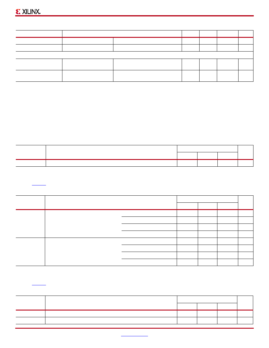
Table 48: CRC Block Switching Characteristics
Symbol
Description
Speed Grade
Units
-3
-2
-1
FCRC
CRCCLK maximum frequency
325
270
MHz
Table 49: Maximum Ethernet MAC Performance
Symbol
Description
Conditions
Speed Grade
Units
-3
-2
-1
FTEMACCLIENT
Client interface maximum frequency
10 Mb/s – 8-bit width
1.25
MHz
100 Mb/s – 8-bit width
12.5
MHz
1000 Mb/s – 8-bit width
125
MHz
2000 Mb/s – 16-bit width
125
MHz
FTEMACPHY
Physical interface maximum frequency
10 Mb/s – 4-bit width
2.5
MHz
100 Mb/s – 4-bit width
25
MHz
1000 Mb/s – 8-bit width
125
MHz
2000 Mb/s – 8-bit width
250
MHz
Table 50: Maximum Performance for PCI Express Designs
Symbol
Description
Speed Grade
Units
-3
-2
-1
FPCIECORE
Core clock maximum frequency
250
MHz
FPCIEUSER
User clock maximum frequency
250
MHz
Table 47: GTX_DUAL Tile Receiver Switching Characteristics (Cont’d)
Symbol
Description
Min
Typ
Max
Units
相关PDF资料 |
PDF描述 |
|---|---|
| XC5VLX85T-3FF1136C | IC FPGA VIRTEX-5 85K 1136FBGA |
| XC5VLX85T-2FFG1136I | IC FPGA VIRTEX-5 85K 1136FBGA |
| XC5VLX85T-2FF1136I | IC FPGA VIRTEX-5 85K 1136FBGA |
| XC2V3000-5BG728I | IC FPGA VIRTEX-II 728PBGA |
| XC6VLX130T-3FFG784C | IC FPGA VIRTEX 6 128K 484FFGBGA |
相关代理商/技术参数 |
参数描述 |
|---|---|
| XC5VLX85T-X1FF1136C | 制造商:Xilinx 功能描述: |
| XC5VLX85T-X1FFG1136C | 制造商:Xilinx 功能描述: |
| XC5VLX85-X1FF1153C | 制造商:Xilinx 功能描述: |
| XC5VLX85-X1FF676C | 制造商:Xilinx 功能描述: |
| XC5VLX85-X1FFG1153C | 制造商:Xilinx 功能描述: |
发布紧急采购,3分钟左右您将得到回复。