参数资料
| 型号: | XC5VLX85T-3FFG1136C |
| 厂商: | Xilinx Inc |
| 文件页数: | 7/91页 |
| 文件大小: | 0K |
| 描述: | IC FPGA VIRTEX-5 85K 1136FBGA |
| 产品变化通告: | Step Intro and Pkg Change 11/March/2008 |
| 标准包装: | 1 |
| 系列: | Virtex®-5 LXT |
| LAB/CLB数: | 6480 |
| 逻辑元件/单元数: | 82944 |
| RAM 位总计: | 3981312 |
| 输入/输出数: | 480 |
| 电源电压: | 0.95 V ~ 1.05 V |
| 安装类型: | 表面贴装 |
| 工作温度: | 0°C ~ 85°C |
| 封装/外壳: | 1136-BBGA,FCBGA |
| 供应商设备封装: | 1136-FCBGA |
| 配用: | 568-5088-ND - BOARD DEMO DAC1408D750 |
第1页第2页第3页第4页第5页第6页当前第7页第8页第9页第10页第11页第12页第13页第14页第15页第16页第17页第18页第19页第20页第21页第22页第23页第24页第25页第26页第27页第28页第29页第30页第31页第32页第33页第34页第35页第36页第37页第38页第39页第40页第41页第42页第43页第44页第45页第46页第47页第48页第49页第50页第51页第52页第53页第54页第55页第56页第57页第58页第59页第60页第61页第62页第63页第64页第65页第66页第67页第68页第69页第70页第71页第72页第73页第74页第75页第76页第77页第78页第79页第80页第81页第82页第83页第84页第85页第86页第87页第88页第89页第90页第91页
Virtex-5 FPGA Data Sheet: DC and Switching Characteristics
DS202 (v5.3) May 5, 2010
Product Specification
15
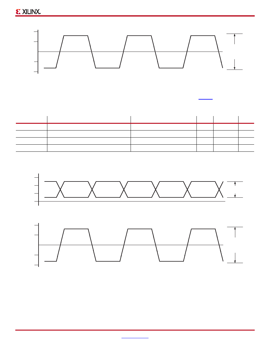
Table 29 summarizes the DC specifications of the clock input of the GTP_DUAL tile. Figure 3 shows the single-ended input
voltage swing. Figure 4 shows the peak-to-peak differential clock input voltage swing. Consult UG196: Virtex-5 FPGA
RocketIO GTP Transceiver User Guide for further details.
X-Ref Target - Figure 2
Figure 2: Peak-to-Peak Differential Output Voltage
Table 29: GTP_DUAL Tile Clock DC Input Specifications(1)
Symbol
DC Parameter
Conditions
Min
Typ
Max
Units
VIDIFF
Differential peak-to-peak input voltage
200
800
2000
mV
VISE
Single-ended input voltage
100
400
1000
mV
RIN
Differential input resistance
80
105
130
Ω
CEXT
Required external AC coupling capacitor
75
100
200
nF
Notes:
1.
VMIN = 0V and VMAX = 1200mV
X-Ref Target - Figure 3
Figure 3: Single-Ended Clock Input Voltage Swing Peak-to-Peak
X-Ref Target - Figure 4
Figure 4: Differential Clock Input Voltage Swing Peak-to-Peak
0
+V
–V
P–N
DVPPOUT
ds202_02_081809
0
+V
P
N
VISE
ds202_03_052708
0
+V
–V
P – N
VIDIFF
ds202_04_052708
相关PDF资料 |
PDF描述 |
|---|---|
| XC5VLX85T-3FF1136C | IC FPGA VIRTEX-5 85K 1136FBGA |
| XC5VLX85T-2FFG1136I | IC FPGA VIRTEX-5 85K 1136FBGA |
| XC5VLX85T-2FF1136I | IC FPGA VIRTEX-5 85K 1136FBGA |
| XC2V3000-5BG728I | IC FPGA VIRTEX-II 728PBGA |
| XC6VLX130T-3FFG784C | IC FPGA VIRTEX 6 128K 484FFGBGA |
相关代理商/技术参数 |
参数描述 |
|---|---|
| XC5VLX85T-X1FF1136C | 制造商:Xilinx 功能描述: |
| XC5VLX85T-X1FFG1136C | 制造商:Xilinx 功能描述: |
| XC5VLX85-X1FF1153C | 制造商:Xilinx 功能描述: |
| XC5VLX85-X1FF676C | 制造商:Xilinx 功能描述: |
| XC5VLX85-X1FFG1153C | 制造商:Xilinx 功能描述: |
发布紧急采购,3分钟左右您将得到回复。