参数资料
| 型号: | XC5VLX85T-3FFG1136C |
| 厂商: | Xilinx Inc |
| 文件页数: | 5/91页 |
| 文件大小: | 0K |
| 描述: | IC FPGA VIRTEX-5 85K 1136FBGA |
| 产品变化通告: | Step Intro and Pkg Change 11/March/2008 |
| 标准包装: | 1 |
| 系列: | Virtex®-5 LXT |
| LAB/CLB数: | 6480 |
| 逻辑元件/单元数: | 82944 |
| RAM 位总计: | 3981312 |
| 输入/输出数: | 480 |
| 电源电压: | 0.95 V ~ 1.05 V |
| 安装类型: | 表面贴装 |
| 工作温度: | 0°C ~ 85°C |
| 封装/外壳: | 1136-BBGA,FCBGA |
| 供应商设备封装: | 1136-FCBGA |
| 配用: | 568-5088-ND - BOARD DEMO DAC1408D750 |
第1页第2页第3页第4页当前第5页第6页第7页第8页第9页第10页第11页第12页第13页第14页第15页第16页第17页第18页第19页第20页第21页第22页第23页第24页第25页第26页第27页第28页第29页第30页第31页第32页第33页第34页第35页第36页第37页第38页第39页第40页第41页第42页第43页第44页第45页第46页第47页第48页第49页第50页第51页第52页第53页第54页第55页第56页第57页第58页第59页第60页第61页第62页第63页第64页第65页第66页第67页第68页第69页第70页第71页第72页第73页第74页第75页第76页第77页第78页第79页第80页第81页第82页第83页第84页第85页第86页第87页第88页第89页第90页第91页
Virtex-5 FPGA Data Sheet: DC and Switching Characteristics
DS202 (v5.3) May 5, 2010
Product Specification
13
GTP_DUAL Tile Specifications
GTP_DUAL Tile DC Characteristics
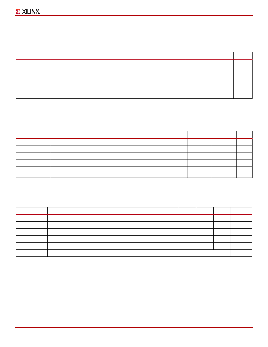
Table 24: Absolute Maximum Ratings for GTP_DUAL Tiles
Symbol
Description
Units
MGTAVCCPLL
Analog supply voltage for the GTP_DUAL shared PLL relative to GND
–0.5 to 1.32
V
MGTAVTTTX
Analog supply voltage for the GTP_DUAL transmitters relative to GND
–0.5 to 1.32
V
MGTAVTTRX
Analog supply voltage for the GTP_DUAL receivers relative to GND
–0.5 to 1.32
V
MGTAVCC
Analog supply voltage for the GTP_DUAL common circuits relative to GND
–0.5 to 1.1
V
MGTAVTTRXC
Analog supply voltage for the resistor calibration circuit of the GTP_DUAL
column
–0.5 to 1.32
V
Notes:
1.
Stresses beyond those listed under Absolute Maximum Ratings might cause permanent damage to the device. These are stress ratings only,
and functional operation of the device at these or any other conditions beyond those listed under Operating Conditions is not implied.
Exposure to Absolute Maximum Ratings conditions for extended periods of time might affect device reliability.
Table 25: Recommended Operating Conditions for GTP_DUAL Tiles(1)(2)
Symbol
Description
Min
Max
Units
MGTAVCCPLL(1)
Analog supply voltage for the GTP_DUAL shared PLL relative to GND
1.14
1.26
V
MGTAVTTTX(1)
Analog supply voltage for the GTP_DUAL transmitters relative to GND
1.14
1.26
V
MGTAVTTRX(1)
Analog supply voltage for the GTP_DUAL receivers relative to GND
1.14
1.26
V
MGTAVCC(1)
Analog supply voltage for the GTP_DUAL common circuits relative to GND
0.95
1.05
V
MGTAVTTRXC(1) Analog supply voltage for the resistor calibration circuit of the GTP_DUAL
column
1.14
1.26
V
Notes:
1.
Each voltage listed requires the filter circuit described in UG196: Virtex-5 FPGA RocketIO GTP Transceiver User Guide.
2.
Voltages are specified for the temperature range of TJ = –40°C to +100°C.
Table 26: DC Characteristics Over Recommended Operating Conditions for GTP_DUAL Tiles(1)
Symbol
Description
Min
Typ
Max
Units
IMGTAVTTTX
GTP_DUAL tile transmitter termination supply current(2)
71
90
mA
IMGTAVCCPLL
GTP_DUAL tile shared PLL supply current
36
60
mA
IMGTAVTTRXC
GTP_DUAL tile resistor termination calibration supply current
0.1
0.5
mA
IMGTAVTTRX
GTP_DUAL tile receiver termination supply current(3)
0.1
0.5
mA
IMGTAVCC
GTP_DUAL tile internal analog supply current
56
110
mA
MGTRREF
Precision reference resistor for internal calibration termination
49.9 ± 1% tolerance
Ω
Notes:
1.
Typical values are specified at nominal voltage, 25°C, with a 3.2 Gb/s line rate.
2.
ICC numbers are given per GTP_DUAL tile with both GTP transceivers operating with default settings.
3.
AC coupled TX/RX link.
相关PDF资料 |
PDF描述 |
|---|---|
| XC5VLX85T-3FF1136C | IC FPGA VIRTEX-5 85K 1136FBGA |
| XC5VLX85T-2FFG1136I | IC FPGA VIRTEX-5 85K 1136FBGA |
| XC5VLX85T-2FF1136I | IC FPGA VIRTEX-5 85K 1136FBGA |
| XC2V3000-5BG728I | IC FPGA VIRTEX-II 728PBGA |
| XC6VLX130T-3FFG784C | IC FPGA VIRTEX 6 128K 484FFGBGA |
相关代理商/技术参数 |
参数描述 |
|---|---|
| XC5VLX85T-X1FF1136C | 制造商:Xilinx 功能描述: |
| XC5VLX85T-X1FFG1136C | 制造商:Xilinx 功能描述: |
| XC5VLX85-X1FF1153C | 制造商:Xilinx 功能描述: |
| XC5VLX85-X1FF676C | 制造商:Xilinx 功能描述: |
| XC5VLX85-X1FFG1153C | 制造商:Xilinx 功能描述: |
发布紧急采购,3分钟左右您将得到回复。