参数资料
| 型号: | XCS20-3PQ208C |
| 厂商: | Xilinx Inc |
| 文件页数: | 13/83页 |
| 文件大小: | 0K |
| 描述: | IC FPGA 5V C-TEMP 208-PQFP |
| 产品变化通告: | Spartan,Virtex FPGA/SCD Discontinuation 18/Oct/2010 |
| 标准包装: | 24 |
| 系列: | Spartan® |
| LAB/CLB数: | 400 |
| 逻辑元件/单元数: | 950 |
| RAM 位总计: | 12800 |
| 输入/输出数: | 160 |
| 门数: | 20000 |
| 电源电压: | 4.75 V ~ 5.25 V |
| 安装类型: | 表面贴装 |
| 工作温度: | 0°C ~ 85°C |
| 封装/外壳: | 208-BFQFP |
| 供应商设备封装: | 208-PQFP(28x28) |
第1页第2页第3页第4页第5页第6页第7页第8页第9页第10页第11页第12页当前第13页第14页第15页第16页第17页第18页第19页第20页第21页第22页第23页第24页第25页第26页第27页第28页第29页第30页第31页第32页第33页第34页第35页第36页第37页第38页第39页第40页第41页第42页第43页第44页第45页第46页第47页第48页第49页第50页第51页第52页第53页第54页第55页第56页第57页第58页第59页第60页第61页第62页第63页第64页第65页第66页第67页第68页第69页第70页第71页第72页第73页第74页第75页第76页第77页第78页第79页第80页第81页第82页第83页
Spartan and Spartan-XL FPGA Families Data Sheet
20
DS060 (v2.0) March 1, 2013
Product Specification
R
Product Obsolete/Under Obsolescence
On-Chip Oscillator
Spartan/XL devices include an internal oscillator. This oscil-
lator is used to clock the power-on time-out, for configura-
tion memory clearing, and as the source of CCLK in Master
configuration mode. The oscillator runs at a nominal 8 MHz
frequency that varies with process, VCC, and temperature.
The output frequency falls between 4 MHz and 10 MHz.
The oscillator output is optionally available after configura-
tion. Any two of four resynchronized taps of a built-in divider
are also available. These taps are at the fourth, ninth, four-
teenth and nineteenth bits of the divider. Therefore, if the
primary oscillator output is running at the nominal 8 MHz,
the user has access to an 8-MHz clock, plus any two of
500 kHz, 16 kHz, 490 Hz and 15 Hz. These frequencies
can vary by as much as -50% or +25%.
These signals can be accessed by placing the OSC4 library
element in a schematic or in HDL code. The oscillator is
automatically disabled after configuration if the OSC4 sym-
bol is not used in the design.
Global Signals: GSR and GTS
Global Set/Reset
A separate Global Set/Reset line, as shown in Figure 3,
page 5 for the CLB and Figure 5, page 6 for the IOB, sets or
clears each flip-flop during power-up, reconfiguration, or
when a dedicated Reset net is driven active. This global net
(GSR) does not compete with other routing resources; it
uses a dedicated distribution network.
Each flip-flop is configured as either globally set or reset in
the same way that the local set/reset (SR) is specified.
Therefore, if a flip-flop is set by SR, it is also set by GSR.
Similarly, if in reset mode, it is reset by both SR and GSR.
GSR can be driven from any user-programmable pin as a
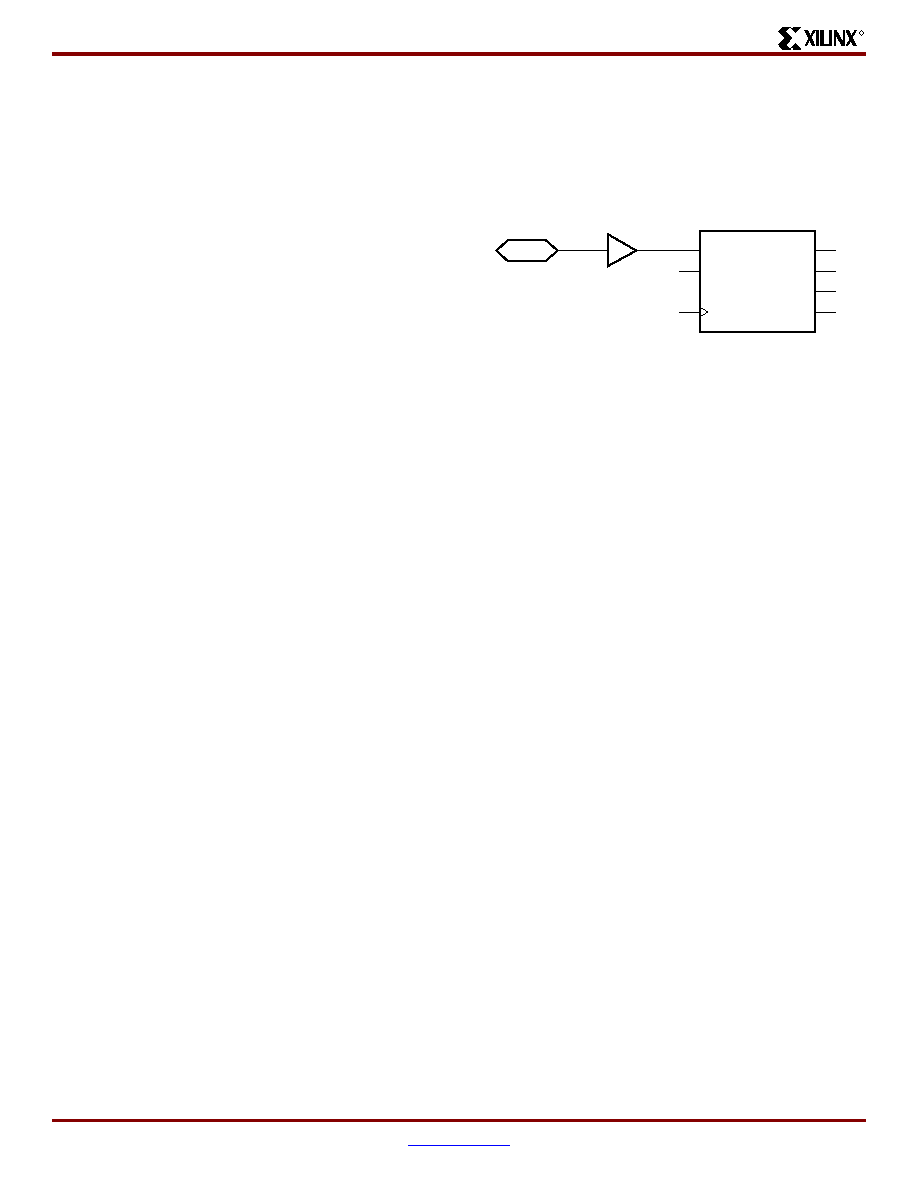
global reset input. To use this global net, place an input pad
and input buffer in the schematic or HDL code, driving the
GSR pin of the STARTUP symbol. (See Figure 19.) A spe-
cific pin location can be assigned to this input using a LOC
attribute or property, just as with any other user-program-
mable pad. An inverter can optionally be inserted after the
input buffer to invert the sense of the GSR signal. Alterna-
tively, GSR can be driven from any internal node.
Global 3-State
A separate Global 3-state line (GTS) as shown in Figure 6,
page 7 forces all FPGA outputs to the high-impedance
state, unless boundary scan is enabled and is executing an
EXTEST instruction. GTS does not compete with other rout-
ing resources; it uses a dedicated distribution network.
GTS can be driven from any user-programmable pin as a
global 3-state input. To use this global net, place an input
pad and input buffer in the schematic or HDL code, driving
the GTS pin of the STARTUP symbol. This is similar to what
is shown in Figure 19 for GSR except the IBUF would be
connected to GTS. A specific pin location can be assigned
to this input using a LOC attribute or property, just as with
any other user-programmable pad. An inverter can option-
ally be inserted after the input buffer to invert the sense of
the Global 3-state signal. Alternatively, GTS can be driven
from any internal node.
Boundary Scan
The "bed of nails" has been the traditional method of testing
electronic assemblies. This approach has become less
appropriate, due to closer pin spacing and more sophisti-
cated assembly methods like surface-mount technology
and multi-layer boards. The IEEE Boundary Scan Standard
1149.1 was developed to facilitate board-level testing of
electronic assemblies. Design and test engineers can
embed a standard test logic structure in their device to
achieve high fault coverage for I/O and internal logic. This
structure is easily implemented with a four-pin interface on
any boundary scan compatible device. IEEE 1149.1-com-
patible devices may be serial daisy-chained together, con-
nected in parallel, or a combination of the two.
The Spartan and Spartan-XL families implement IEEE
1149.1-compatible
BYPASS,
PRELOAD/SAMPLE
and
EXTEST boundary scan instructions. When the boundary
scan configuration option is selected, three normal user I/O
pins become dedicated inputs for these functions. Another
user output pin becomes the dedicated boundary scan out-
put. The details of how to enable this circuitry are covered
later in this section.
By exercising these input signals, the user can serially load
commands and data into these devices to control the driving
of their outputs and to examine their inputs. This method is
an improvement over bed-of-nails testing. It avoids the need
to over-drive device outputs, and it reduces the user inter-
face to four pins. An optional fifth pin, a reset for the control
logic, is described in the standard but is not implemented in
the Spartan/XL devices.
The dedicated on-chip logic implementing the IEEE 1149.1
functions includes a 16-state machine, an instruction regis-
ter and a number of data registers. The functional details
can be found in the IEEE 1149.1 specification and are also
discussed in the Xilinx application note: "Boundary Scan in
FPGA Devices."
Figure 19: Symbols for Global Set/Reset
PAD
IBUF
GSR
GTS
CLK
DONEIN
Q1, Q4
Q2
Q3
STARTUP
DS060_19_080400
相关PDF资料 |
PDF描述 |
|---|---|
| XCS10XL-5VQ100C | IC FPGA 3.3V C-TEMP 100-VQFP |
| XCS10XL-5TQ144C | IC FPGA 3.3V C-TEMP 144-TQFP |
| IDT7015S15J | IC SRAM 72KBIT 15NS 68PLCC |
| FMM43DSEH-S243 | CONN EDGECARD 86POS .156 EYELET |
| IDT71V67803S166BG | IC SRAM 9MBIT 166MHZ 119BGA |
相关代理商/技术参数 |
参数描述 |
|---|---|
| XCS203PQ208C0600 | 制造商:Xilinx 功能描述: |
| XCS20-3PQ208I | 功能描述:IC FPGA 5V I-TEMP 208-PQFP RoHS:否 类别:集成电路 (IC) >> 嵌入式 - FPGA(现场可编程门阵列) 系列:Spartan® 标准包装:1 系列:Kintex-7 LAB/CLB数:25475 逻辑元件/单元数:326080 RAM 位总计:16404480 输入/输出数:350 门数:- 电源电压:0.97 V ~ 1.03 V 安装类型:表面贴装 工作温度:0°C ~ 85°C 封装/外壳:900-BBGA,FCBGA 供应商设备封装:900-FCBGA(31x31) 其它名称:122-1789 |
| XCS20-3PQ240C | 制造商:XILINX 制造商全称:XILINX 功能描述:Spartan and Spartan-XL Families Field Programmable Gate Arrays |
| XCS20-3PQ240I | 制造商:XILINX 制造商全称:XILINX 功能描述:Spartan and Spartan-XL FPGA |
| XCS20-3PQ256C | 制造商:XILINX 制造商全称:XILINX 功能描述:Spartan and Spartan-XL Families Field Programmable Gate Arrays |
发布紧急采购,3分钟左右您将得到回复。