- 您现在的位置:买卖IC网 > PDF目录225573 > XCV200-6FGG456I (XILINX INC) FPGA, 1176 CLBS, 236666 GATES, 333 MHz, PBGA456 PDF资料下载
参数资料
| 型号: | XCV200-6FGG456I |
| 厂商: | XILINX INC |
| 元件分类: | FPGA |
| 英文描述: | FPGA, 1176 CLBS, 236666 GATES, 333 MHz, PBGA456 |
| 封装: | FBGA-456 |
| 文件页数: | 14/24页 |
| 文件大小: | 167K |
| 代理商: | XCV200-6FGG456I |
Virtex 2.5 V Field Programmable Gate Arrays
R
DS003-3 (v3.2) September 10, 2002
Module 3 of 4
Production Product Specification
1-800-255-7778
21
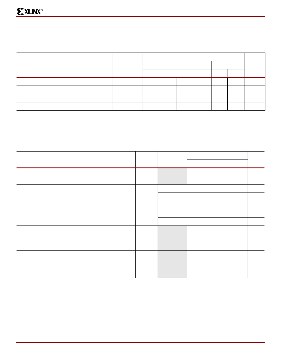
DLL Timing Parameters
All devices are 100 percent functionally tested. Because of the difficulty in directly measuring many internal timing
parameters, those parameters are derived from benchmark timing patterns. The following guidelines reflect worst-case
values across the recommended operating conditions.
DLL Clock Tolerance, Jitter, and Phase Information
All DLL output jitter and phase specifications determined through statistical measurement at the package pins using a clock
mirror configuration and matched drivers.
Description
Symbol
Speed Grade
Units
-6
-5
-4
Min
Max
Min
Max
Min
Max
Input Clock Frequency (CLKDLLHF)
FCLKINHF
60
200
60
180
60
180
MHz
Input Clock Frequency (CLKDLL)
FCLKINLF
25
100
25
90
25
90
MHz
Input Clock Pulse Width (CLKDLLHF)
TDLLPWHF
2.0
-
2.4
-
2.4
-
ns
Input Clock Pulse Width (CLKDLL)
TDLLPWLF
2.5
-
3.0
-
ns
Notes:
1.
All specifications correspond to Commercial Operating Temperatures (0°C to + 85°C).
Description
Symbol
F
CLKIN
CLKDLLHF
CLKDLL
Units
Min
Max
Min
Max
Input Clock Period Tolerance
TIPTOL
-
1.0
-
1.0
ns
Input Clock Jitter Tolerance (Cycle to Cycle)
TIJITCC
-
± 150
-
± 300
ps
Time Required for DLL to Acquire Lock
TLOCK
> 60 MHz
-
20
-
20
s
50 - 60 MHz
-
25
s
40 - 50 MHz
-
50
s
30 - 40 MHz
-
90
s
25 - 30 MHz
-
120
s
Output Jitter (cycle-to-cycle) for any DLL Clock Output(1)
TOJITCC
± 60
ps
Phase Offset between CLKIN and CLKO(2)
TPHIO
± 100
ps
Phase Offset between Clock Outputs on the DLL(3)
TPHOO
± 140
ps
Maximum Phase Difference between CLKIN and
CLKO(4)
TPHIOM
± 160
ps
Maximum Phase Difference between Clock Outputs on
the DLL(5)
TPHOOM
± 200
ps
Notes:
1.
Output Jitter is cycle-to-cycle jitter measured on the DLL output clock, excluding input clock jitter.
2.
Phase Offset between CLKIN and CLKO is the worst-case fixed time difference between rising edges of CLKIN and CLKO,
excluding Output Jitter and input clock jitter.
3.
Phase Offset between Clock Outputs on the DLL is the worst-case fixed time difference between rising edges of any two DLL
outputs, excluding Output Jitter and input clock jitter.
4.
Maximum Phase Difference between CLKIN an CLKO is the sum of Output Jitter and Phase Offset between CLKIN and CLKO,
or the greatest difference between CLKIN and CLKO rising edges due to DLL alone (excluding input clock jitter).
5.
Maximum Phase DIfference between Clock Outputs on the DLL is the sum of Output JItter and Phase Offset between any DLL
clock outputs, or the greatest difference between any two DLL output rising edges sue to DLL alone (excluding input clock jitter).
6.
All specifications correspond to Commercial Operating Temperatures (0°C to +85°C).
相关PDF资料 |
PDF描述 |
|---|---|
| XCV200-6PQG240I | FPGA, 1176 CLBS, 236666 GATES, 333 MHz, PQFP240 |
| XCV200-6BGG256I | FPGA, 1176 CLBS, 236666 GATES, 333 MHz, PBGA256 |
| XCV200-6BGG352I | FPGA, 1176 CLBS, 236666 GATES, 333 MHz, PBGA352 |
| XD010-04S-D4FY | 350 MHz - 600 MHz RF/MICROWAVE WIDE BAND HIGH POWER AMPLIFIER |
| XF2B-2145-31A | 21 CONTACT(S), FEMALE, STRAIGHT FFC/FPC CONNECTOR, SOLDER |
相关代理商/技术参数 |
参数描述 |
|---|---|
| XCV200-6PQ240C | 功能描述:IC FPGA 2.5V C-TEMP 240-PQFP RoHS:否 类别:集成电路 (IC) >> 嵌入式 - FPGA(现场可编程门阵列) 系列:Virtex® 标准包装:1 系列:Kintex-7 LAB/CLB数:25475 逻辑元件/单元数:326080 RAM 位总计:16404480 输入/输出数:350 门数:- 电源电压:0.97 V ~ 1.03 V 安装类型:表面贴装 工作温度:0°C ~ 85°C 封装/外壳:900-BBGA,FCBGA 供应商设备封装:900-FCBGA(31x31) 其它名称:122-1789 |
| XCV200-6PQ240I | 制造商:XILINX 制造商全称:XILINX 功能描述:Field Programmable Gate Arrays |
| XCV200-6PQG240C | 制造商:Xilinx 功能描述:FPGA VIRTEX 236.666K GATES 5292 CELLS 333MHZ 0.22UM 2.5V 240 - Trays |
| XCV200E | 制造商:XILINX 制造商全称:XILINX 功能描述:Field Programmable Gate Arrays |
| XCV200E-6BG240C | 制造商:XILINX 制造商全称:XILINX 功能描述:Virtex⑩-E 1.8 V Field Programmable Gate Arrays |
发布紧急采购,3分钟左右您将得到回复。