- 您现在的位置:买卖IC网 > PDF目录225573 > XCV200-6FGG456I (XILINX INC) FPGA, 1176 CLBS, 236666 GATES, 333 MHz, PBGA456 PDF资料下载
参数资料
| 型号: | XCV200-6FGG456I |
| 厂商: | XILINX INC |
| 元件分类: | FPGA |
| 英文描述: | FPGA, 1176 CLBS, 236666 GATES, 333 MHz, PBGA456 |
| 封装: | FBGA-456 |
| 文件页数: | 5/24页 |
| 文件大小: | 167K |
| 代理商: | XCV200-6FGG456I |
Virtex 2.5 V Field Programmable Gate Arrays
R
DS003-3 (v3.2) September 10, 2002
Module 3 of 4
Production Product Specification
1-800-255-7778
13
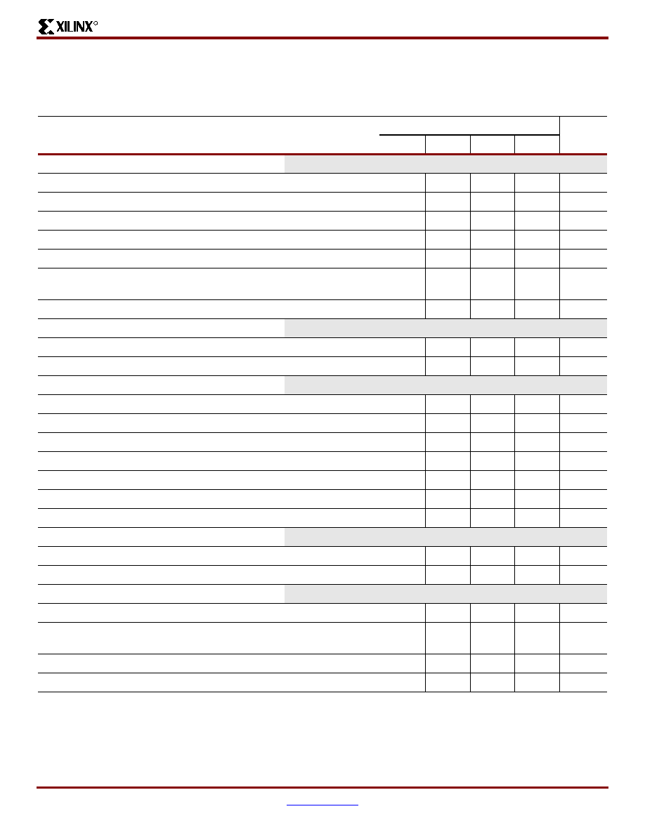
CLB Switching Characteristics
Delays originating at F/G inputs vary slightly according to the input used. The values listed below are worst-case. Precise
values are provided by the timing analyzer.
Description
Symbol
Speed Grade
Units
Min
-6-5-4
Combinatorial Delays
4-input function: F/G inputs to X/Y outputs
TILO
0.29
0.6
0.7
0.8
ns, max
5-input function: F/G inputs to F5 output
TIF5
0.32
0.7
0.8
0.9
ns, max
5-input function: F/G inputs to X output
TIF5X
0.36
0.8
1.0
ns, max
6-input function: F/G inputs to Y output via F6 MUX
TIF6Y
0.44
0.9
1.0
1.2
ns, max
6-input function: F5IN input to Y output
TF5INY
0.17
0.32
0.36
0.42
ns, max
Incremental delay routing through transparent latch
to XQ/YQ outputs
TIFNCTL
0.31
0.7
0.8
ns, max
BY input to YB output
TBYYB
0.27
0.53
0.6
0.7
ns, max
Sequential Delays
FF Clock CLK to XQ/YQ outputs
TCKO
0.54
1.1
1.2
1.4
ns, max
Latch Clock CLK to XQ/YQ outputs
TCKLO
0.6
1.2
1.4
1.6
ns, max
Setup and Hold Times before/after Clock CLK(1)
Setup Time / Hold Time
4-input function: F/G Inputs
TICK/TCKI
0.6 / 0
1.2 / 0
1.4 / 0
1.5 / 0
ns, min
5-input function: F/G inputs
TIF5CK/TCKIF5
0.7 / 0
1.3 / 0
1.5 / 0
1.7 / 0
ns, min
6-input function: F5IN input
TF5INCK/TCKF5IN
0.46 / 0
1.0 / 0
1.1 / 0
1.2 / 0
ns, min
6-input function: F/G inputs via F6 MUX
TIF6CK/TCKIF6
0.8 / 0
1.5 / 0
1.7 / 0
1.9 / 0
ns, min
BX/BY inputs
TDICK/TCKDI
0.30 / 0
0.6 / 0
0.7 / 0
0.8 / 0
ns, min
CE input
TCECK/TCKCE
0.37 / 0
0.8 / 0
0.9 / 0
1.0 / 0
ns, min
SR/BY inputs (synchronous)
TRCKTCKR
0.33 / 0
0.7 / 0
0.8 / 0
0.9 / 0
ns, min
Clock CLK
Minimum Pulse Width, High
TCH
0.8
1.5
1.7
2.0
ns, min
Minimum Pulse Width, Low
TCL
0.8
1.5
1.7
2.0
ns, min
Set/Reset
Minimum Pulse Width, SR/BY inputs
TRPW
1.3
2.5
2.8
3.3
ns, min
Delay from SR/BY inputs to XQ/YQ outputs
(asynchronous)
TRQ
0.54
1.1
1.3
1.4
ns, max
Delay from GSR to XQ/YQ outputs
TIOGSRQ
4.9
9.7
10.9
12.5
ns, max
Toggle Frequency (MHz) (for export control)
FTOG (MHz)
625
333
294
250
MHz
Notes:
1.
A Zero "0" Hold Time listing indicates no hold time or a negative hold time. Negative values cannot be guaranteed "best-case", but
if a "0" is listed, there is no positive hold time.
相关PDF资料 |
PDF描述 |
|---|---|
| XCV200-6PQG240I | FPGA, 1176 CLBS, 236666 GATES, 333 MHz, PQFP240 |
| XCV200-6BGG256I | FPGA, 1176 CLBS, 236666 GATES, 333 MHz, PBGA256 |
| XCV200-6BGG352I | FPGA, 1176 CLBS, 236666 GATES, 333 MHz, PBGA352 |
| XD010-04S-D4FY | 350 MHz - 600 MHz RF/MICROWAVE WIDE BAND HIGH POWER AMPLIFIER |
| XF2B-2145-31A | 21 CONTACT(S), FEMALE, STRAIGHT FFC/FPC CONNECTOR, SOLDER |
相关代理商/技术参数 |
参数描述 |
|---|---|
| XCV200-6PQ240C | 功能描述:IC FPGA 2.5V C-TEMP 240-PQFP RoHS:否 类别:集成电路 (IC) >> 嵌入式 - FPGA(现场可编程门阵列) 系列:Virtex® 标准包装:1 系列:Kintex-7 LAB/CLB数:25475 逻辑元件/单元数:326080 RAM 位总计:16404480 输入/输出数:350 门数:- 电源电压:0.97 V ~ 1.03 V 安装类型:表面贴装 工作温度:0°C ~ 85°C 封装/外壳:900-BBGA,FCBGA 供应商设备封装:900-FCBGA(31x31) 其它名称:122-1789 |
| XCV200-6PQ240I | 制造商:XILINX 制造商全称:XILINX 功能描述:Field Programmable Gate Arrays |
| XCV200-6PQG240C | 制造商:Xilinx 功能描述:FPGA VIRTEX 236.666K GATES 5292 CELLS 333MHZ 0.22UM 2.5V 240 - Trays |
| XCV200E | 制造商:XILINX 制造商全称:XILINX 功能描述:Field Programmable Gate Arrays |
| XCV200E-6BG240C | 制造商:XILINX 制造商全称:XILINX 功能描述:Virtex⑩-E 1.8 V Field Programmable Gate Arrays |
发布紧急采购,3分钟左右您将得到回复。